The Saturn PCB Toolkit is a handy resource, by the way: Saturn PCB Toolkit - Saturn PCB Design | Saturn PCB Design
Tom
Tom
7mm between PE and N; 7mm between PE and L.
If Cat. II could be reduce to 3mm.
@Jean-Paul
I‘ve learned something different with mounting holes in PCB! More moment on the screw and you‘ll explode the plated hole.
If I remains there is something in Navy engineering books?!
JP
If Cat. II could be reduce to 3mm.
@Jean-Paul
I‘ve learned something different with mounting holes in PCB! More moment on the screw and you‘ll explode the plated hole.
If I remains there is something in Navy engineering books?!
JP
7mm between PE and N; 7mm between PE and L.
If Cat. II could be reduce to 3mm.
Thank you. That was my understanding as well.
Tom
@Jean-Paul
I‘ve learned something different with mounting holes in PCB! More moment on the screw and you‘ll explode the plated hole.
Since I am not in the EU regulation board I sleep well with all my PCB's having metallized holes and 6 mm spacing. In case lightning strikes and they all explode so be it.
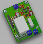
That board looks good!
Last edited:
I try to remember to not be afraid to move the mounting holes somewhere else. After all, you can always mount stuff with hawt snot; or mount it on three legs - the fourth being a stud.
Remember that having them not in a regular pattern makes it only harder for you to drill the holes. It is DIY and not CAD/CAM for most. It also makes sense to use them near the more heavy parts like transformers. Without even looking at regulations my opinion is that a device should function 100% after falling from 30 cm height. When one designs and also repairs stuff such design imperfections influence ones skills on mechanical strength. Many if not most possible issues can be omitted by design. I recall a certain Japanese brand that designed measurement equipment with the mains transformer (PCB mounted) on a PCB that was itself mounted upside down. Just placing the device a bit too careless on the bench would cause the transformer to break the PCB.
Some DIYers omit the mounting holes and mount stuff with melting glue on wooden panels so any mounting hole in DIY designs is a victory to safety and the reputation of DIY 🙂
Some DIYers omit the mounting holes and mount stuff with melting glue on wooden panels so any mounting hole in DIY designs is a victory to safety and the reputation of DIY 🙂
Last edited:
Oh I am not the heathen that will move them to irregular positions. If I am moving any to other positions, they will always be easily alignable, eg diagonals between other holes or easily measured from them. No half mm's
That’s why I have 6 of them! 😛😱😉…so any mounting hole in DIY designs is a victory to safety and the reputation of DIY 🙂
Ok. Seriously though, yeah, I’ll take a look at JPs solution and study it a bit. Is it usual (or even feasible) to have PCB builders cut ditches like that on the PCB? Is that more expensive to build?
I’m going to also play around with rotating the IRM and see if that frees some overlapping traces.
Thanks for all the help!
Rafa.
It occurs to me that having 2 persons with the same name can be confusing 😉
Anyway, you could of course have the design by JP produced. It seems to cover most aspects very well. Single board design which our committee can only endorse 100%.
If you mean the cutouts, yes these are meanwhile quite normal and AFAIK they don't cost extra or I did not pay attention. As non English speakers we tend to use the term "spacing" or "space" but more accurate would be creepage and clearance as indicated earlier by Tom. Enough "air" between conductors guarantees clearance and it prevents creepage along the surface of the board. They are often an ideal place for dirt to cumulate and they make larger boards less sturdy. Like in every profession jargon and some innovations are invented every now and then of which one can ask if they are worth the trouble.
Creepage is not occurring that much in low voltage designs but if one can one must design stuff to be passively cooled in an enclosed casing. That way dirt and dust can not become conductors. In high voltage applications it can surprise what dirt can cause, just like insects and rodents. Or even a small bubble of air in the isolation of cables.
Last edited by a moderator:
I know Tom [...]
No worries. The standards are not the easiest to read, so I was just double-checking that I was on the same page as everybody else. 🙂
Without even looking at regulations my opinion is that a device should function 100% after falling from 30 cm height.
I agree. If it doesn't survive that, it probably won't survive shipping. Many DIY projects end up in shipping boxes and go across the world after a few years.
Tom
I think some prefer their own standard. Take a good look around you... much stuff that is regulated till death but a longevity of 2 years at max 😀
A nice thing in DIY is one can make stuff as sturdy as one likes. There is cheaply built throw away stuff enough in the world. Personally I like the looks and sturdiness of seventies designs with the quality of todays high res possibilities so I leave the melt glue and wooden panels to others 😉
A nice thing in DIY is one can make stuff as sturdy as one likes. There is cheaply built throw away stuff enough in the world. Personally I like the looks and sturdiness of seventies designs with the quality of todays high res possibilities so I leave the melt glue and wooden panels to others 😉
Last edited:
Is it usual (or even feasible) to have PCB builders cut ditches like that on the PCB? Is that more expensive to build?
You see trenches like that a lot on switching power supplies. If you have 200 boards made you probably have to pay a little extra for internal cutouts, but I would be surprised if the PCB manufacturers that cater to the DIY community charge extra. OSH Park, for example, only cares about the board dimensions.
You may want to check with the PCB manufacturer to see how they want the cutouts defined and which minimum width they support. Most seem to use the FAB layer (Edge.Cuts in KiCAD) but I have dealt with manufacturers who wanted internal cutouts defined in all layers and notes placed within the cutout.
Tom
Isn't that because of high dV/dt values? I would have thought a trench is like a ditch so with a "bottom" and not a complete cutout....They are nice and practical when I put my foot on one of them superior world improving SMPSes. It makes recycling fun.
Last edited:
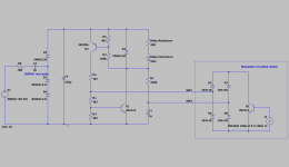
Push-Push switch cirtcuit
OK kids, here is a couple old timer tricks:
1. A simple push-push flip-flop circuit using two inverters or transistors.
2. A simple DC supply directly from the mains.
I have simulated the switch with a diode bridge etc. I assume you understand that this is not part of the circuit.
OK kids, here is a couple old timer tricks:
1. A simple push-push flip-flop circuit using two inverters or transistors.
2. A simple DC supply directly from the mains.
I have simulated the switch with a diode bridge etc. I assume you understand that this is not part of the circuit.
Attachments

Last edited:
Steveu, why don't you send that circuit to Rod Elliott? He may want to update his Project 166 after seeing your schematic. And that would be quite a feather in your cap!
Permesso...
... Anyway, you could of course have the design by JP produced. It seems to cover most aspects very well...
OK kids, here is a couple old timer tricks...
Thanks friends. So, maybe it's worth pointing out a few ideas already mentioned in the original thread: the objective for this project was to learn and create a PCB.
So, I thank mentioning other circuits that fulfill the same roll, but since my idea here is to learn how to do design a PCB, I'll stick with a more or less straightforward and tested circuit which I have already studied and more or less understand (more or less being key here, hence the request for help).
Feel free to discuss other circuits, but I'll be sticking with P166 as unaltered as possible for it to work with the parts and topology being discussed here.
As for the finished PCB, by JP, I am humbled by the fact that you did in a day what took me a couple of weeks to do. Still, I want this to end up with a PCB that, more or less, has the feeling that is was made mostly by me with all the input given. So I will not be using JPs PCB, but taking hints from the design criteria, if that is OK with you.
Still, I have opened the Eagle PCB and the spacing between traces seem to be 3mm, so I must confess I am a bit confused about this "covering most aspects very well" when I am trying to fit 7mm spaces between traces.
So, since this "covers most aspects", can I assume I can aim for 3 ~ 3.5mm distancing between L/N/Chassis traces?
If CAT II is enough, or maybe I just deem this 110V only? I don't seem to be able to fit 7mm spaces, but neither does the relays, or the PSU for that matter, which all have 5.08mm between pins.
Since not even JPs PCB respects this spacing, I believe it is OK?
Thanks again,
Rafa.
- Home
- Amplifiers
- Power Supplies
- PCB: Push on / Push off Mains Switch