....
But I can't figure what Idss I need for CSS JFET.
......
speaking of CCS for input LTP?
why wasting 2SK on that - you need two of them (at least) then you need resistor in series to burn some heat on it, to save JFets of excessive dissipation etc
in the end - ring of two is better CCS and simple enough
BC556, BD140, 3 resistors, simple compute for programmed current (0V65/I=R)
anyhow - simple matching Jig for JFets should tell you what resistor to use for desired programmed current
Pa had his own reasons why he put all JFets in J2 ......... but Papa is also teaching us all the time to use brain, not to copy without thinking
Last edited:
speaking of CCS for input LTP?
why wasting 2SK on that - you need two of them (at least) then you need resistor in series to burn some heat on it, to save JFets of excessive dissipation etc
in the end - ring of two is better CCS and simple enough
BC556, BD140, 3 resistors, simple compute for programmed current (0V65/I=R)
anyhow - simple matching Jig for JFets should tell you what resistor to use for desired programmed current
Pa had his own reasons why he put all JFets in J2 ......... but Papa is also teaching us all the time to use brain, not to copy without thinking
Yes.
Thank you ZM!
I respect your position and common sense.
But I have them and urge feeling to use them is growing in me.. 🙂

I just measured the Idss, since I didn’t use any kind of dropping resistor. Concerning the dissipation, you calculations may very well be accurate, though I can say that they barely get warm on my boards. Regarding output devices, 1.7A x 50v (25v swings) = 85w dissipated across two devices (/2) = 42.5W per device. Or at least that’s the math I’ve been using 😀 A trusted source has suggested 50W as a max for the SS parts, so I’m not too worried. Proof is really at the heat sinks, and mine measure around 53C
Last thing I’ll leave you with - I was told by more than one person (and have read it many places) that 2SK170 for a CCS is a waste. I tend to believe them, but I just had plenty of 170s and figured “what the hell”. 🙂 Point being that I doubt you’d see justifiable performance increase in using them. Can’t say that I have.
Nice distortion spectrum!
At 1.7A current, I suppose the weakest link will be the 2 bonds between MOSFET pins ( d and s), and the silicon die... but it should all be okay at around 45W max. per device.
Thanks! And I am curious to see how it holds up long term. I’d been running the same OS configuration with the store boards for quite a while without problems. Hoping that is an accurate forecast for these new boards 🙂
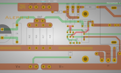
First concept of V2 board with different LTP CCS.
Finally I could double output trace and even widen it a bit.
Also could not resist to experiment with patterns. 🙂
I am not in haste. Those are just experiments.
Finally I could double output trace and even widen it a bit.
Also could not resist to experiment with patterns. 🙂
I am not in haste. Those are just experiments.
Attachments
+1 I may get a set of these myself, they look great!
Thank you for interest! 🙂
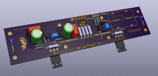
Here it is that same V2 board.
Some thought about simulation from previous page.
Uper and lower output stages are both SJEP120R100 in those.
With AC gain trimmer set to 68.2K and uper output stage source resistor 0.47 Ohm we have 1.375A across it (across resistor).
With same AC gain 68.2K and 0.33 Ohm source resistor we have 1.955A across it.
With same AC gain 68.2K and 0.22 Ohm source resistor we have 2.925A across it!!!
For this simulation safe starting values for AC gain trimmer before solder is:
68.2K - with 0.47 uper source resistor
4.9K - with 0.33 uper source resistor
2.4K - with 0.22 uper source resistor
(for boards with only 2 output stage transistors)
Attachments
upper trimer in Aleph CCS is having some influence on AC gain, but it's primary role is to set Iq
so , do not call it with improper name
so , do not call it with improper name
I would rather agree it sounds misleading.
That resistor is Bias/AC gain.
But yes, the primary role is Bias and that's why we twist that pot.
So I think I should rename this pot on my boards to just simply Bias without mentioning Gain and that's it.
What do you think?
That resistor is Bias/AC gain.
But yes, the primary role is Bias and that's why we twist that pot.
So I think I should rename this pot on my boards to just simply Bias without mentioning Gain and that's it.
What do you think?
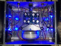
Another Aleph J SemiSouth lives! Literally just finished it and letting it warm up for an hour before I readjust.
Thanks again to Cody for the SemiSouth give away, and as always a huge thanks to Nelson for his generous deigns and contributions to this great forum
Thanks again to Cody for the SemiSouth give away, and as always a huge thanks to Nelson for his generous deigns and contributions to this great forum
Attachments

It’s a new build with 0.22 ohm source resistor values suggested by CodyT.
Last edited:
Thank you for interest! 🙂
Here it is that same V2 board.
Some thought about simulation from previous page.
Uper and lower output stages are both SJEP120R100 in those.
With AC gain trimmer set to 68.2K and uper output stage source resistor 0.47 Ohm we have 1.375A across it (across resistor).
With same AC gain 68.2K and 0.33 Ohm source resistor we have 1.955A across it.
With same AC gain 68.2K and 0.22 Ohm source resistor we have 2.925A across it!!!
For this simulation safe starting values for AC gain trimmer before solder is:
68.2K - with 0.47 uper source resistor
4.9K - with 0.33 uper source resistor
2.4K - with 0.22 uper source resistor
(for boards with only 2 output stage transistors)
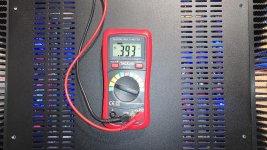
I used 0.22 ohm source resistors in the upper and lower positions and had R27 set at the recommended 68k ohms. When I powered up the amp bias was slightly over 500mv. I quickly lowered the bias to 400mv as I’m only using a 4U/300 chassis.
- Home
- Amplifiers
- Pass Labs
- Semisouth Aleph J?