Very nice! Another nice thing about that LTP bias arrangement – since gate and source are tied together, one could also use a J113 (or other comparable JFET) by flipping the device opposite of the screen.
Very nice! Another nice thing about that LTP bias arrangement – since gate and source are tied together, one could also use a J113 (or other comparable JFET) by flipping the device opposite of the screen.
Didn't thought about it but you are right. 🙂
2SK170/2SJ170 - DGS
J113 - GSD (ON Semi, NXP) But J113 by InterFET is GDS
P.S.: Slightly corrected layout for more pretty symmetry.
Attachments
> can perfectly make that CCS with ring of two bjts
A J113, as used by Nelson, with a source resistor is much simpler, and it is still fully JFET.
Also costs nothing.
And according to Walt Jung, better in performance (Fig. 3B, 8B).
https://audioxpress.com/assets/upload/files/Sources_101_P1.pdf
Cheers,
Patrick
I found this post by Patrick of Walt Junt article about Audio Current Regulator tests.
What do you think if I add JFET cascode to input JFET CCS like in the article?
I also looked what everyone tryed as JFET cascode to 2SK170 and.. Patrick also suggested J111 since about year 2008. 🙂
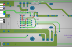
Here is a concept layout.
It may look strange right now.
R8 is a jumper/zero Ohm resistor in this one.
Attachments
I’d consider paralleling the CCS Jfet as an option. Assuming that the current across the one Jfet is the primary concern.
I’d consider paralleling the CCS Jfet as an option. Assuming that the current across the one Jfet is the primary concern.
Cody, did you saw Page 7, "JFET-Based Current Sources and Sinks" and figure 8B?
PSU noise rejection greatly improved for this one.
And if J111 is still a good candidate it would mean adding just one cheap available part.
Ah, I see. I was only thinking about the current, not the noise. It would be interesting to compare the different CCS configurations at the output of the diff pair.
Ah, I see. I was only thinking about the current, not the noise. It would be interesting to compare the different CCS configurations at the output of the diff pair.
ya mean - Tail?
LTP,

Ah yes, the tail. My baaad 😀
Attachments

Last edited:
ygpm, too
ring of two is best you'll ever need , in position as this one (input LTP CCS)
observe Stasis new FE - for Pa - even simple/sole bjt is goodenough as CCS
ZM being Chicken, I always go to double, compensating lack of knowledge, education and courage - with number of parts
though, can't argue if someone have a Fetish for JFets, so even CCS must be JFet one
post 138, you'll recognize T of LTP
About possible Babelfish J interest
"ring of two" , in/according to some sources meaning slightly different circuit - with more symmetry but also with some additional problems
however, I did found same reference for this exact circuit of CCS, and it was easy to remember from first day
later I did found reference to mentioned iteration, but who cares, as long I know what I'm thinking of
Aha! Thanks for pointing me there. And by the way, that’s quite a nice babelfish if I do say so 🙂

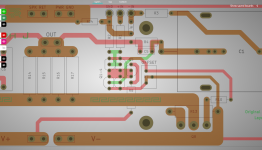
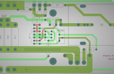
I am not sure if such long traces, allocated to input signal routing to the JEFT's, are going to pose any risk with regard to possible oscillations...? I haven't checked what the input impedance of your design (schematics) is neither...
It is very hard to know if the input section of the PCB will cause any instability due to layout; sometimes even the completely surrounded traces, with a ground fill, could cause issues. I suppose the best is to try and see..???
It is very hard to know if the input section of the PCB will cause any instability due to layout; sometimes even the completely surrounded traces, with a ground fill, could cause issues. I suppose the best is to try and see..???
......quite a nice babelfish if I do say so 🙂
all of them are, by default
I'm ZM
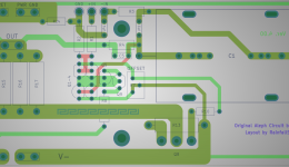
At first I did not understand what you meant.
Then I imagine JP2 shorted and saw a very very long trace.
Well.. maybe not such a good idea.
Then I imagine JP2 shorted and saw a very very long trace.
Well.. maybe not such a good idea.
Have a look at Marantz PCB layouts, CD players and amplifiers. The service manuals are readily available for download.
Compare the original designs (PCB layouts), with Ken Ishiwata (KI) designs (PCB layouts). You will notice the difference in how Ken was routing common returns on "KI" models, and in how he distributed the supply rails.
It was a common understanding that Ken used "specially tuned for audio" parts, to make the KI models sound better compared to the original. But, I think that the PCB layout differences (that not many picked up on) made the biggest - (almost) quantifiable differences.
- Home
- Amplifiers
- Pass Labs
- Semisouth Aleph J?