

Very nice design.
i have always wondered how to get the VAS, drivers and output trannies to mount flat against the heatsink with this type of mounting arrangement since they are different thicknesses. Any tips would be appreciated for future use.
i have always wondered how to get the VAS, drivers and output trannies to mount flat against the heatsink with this type of mounting arrangement since they are different thicknesses. Any tips would be appreciated for future use.
Holes for screws are bigger than screw heads.
Transistors are solidly screwed to the heatsink below,
and PCB is 'levitating' few mm above them.
When soldering transistors to the PCB some kind of precision is needed, better to have heatsink ready and drilled and tapped,
so the holes and heights are aligned well.
That also helps with NOT propagating heat from heatsink to PCB.
Last edited:
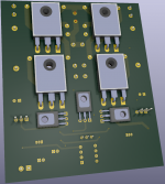
Here is my 4-Layer compact PCB (KiCAD) for the HEXFET version, with 4 output devices.
Very nice work Metal! I like the utilization of SMD components and spade connectors.
Although, I’m have a difficult time uploading the files to JLCPCB. I must be doing something wrong 😕
Very nice design.
i have always wondered how to get the VAS, drivers and output trannies to mount flat against the heatsink with this type of mounting arrangement since they are different thicknesses. Any tips would be appreciated for future use.
As I usually do: first, bend the legs of the transistors to the correct size and angle. Then turn the PCB over on its back and insert the parts into the holes without soldering. Usually the parts fit so well in the holes that you can turn the PCB back without risk of falling out of transistors. Screw all the semiconductors onto the heat sink first then you can solder all of them. (assuming two sided solder points with galvanized holes) I usually use 4 pcs 10mm long spacer between the PCB and heat sink.
Last edited:
thank you guys, comments much appreciated, really 🙂
The trick was to go as compact as 10x8cm to make good use of the 4-layer PCB deal offered by JLCPCB for as low as $8, still be able to hook 4 output devices, place the VAS as close as possible to the output devices pair, and use MELF resistors which I like so much. Of course, DIP-8 for the OPAMP gives the fereedom of changing it any time with a socket soldered in place.
I opted to publish the actual project files because myself I would never build anything for which I have Gerbers only, and I am willing to support the efforts of Daniel and allow other members to have the privilege of modifying the files and making them better too, as I still believe in open-sourcing projects and the value of the community.
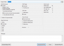
Attached plot settings for your convenience.
The trick was to go as compact as 10x8cm to make good use of the 4-layer PCB deal offered by JLCPCB for as low as $8, still be able to hook 4 output devices, place the VAS as close as possible to the output devices pair, and use MELF resistors which I like so much. Of course, DIP-8 for the OPAMP gives the fereedom of changing it any time with a socket soldered in place.
I opted to publish the actual project files because myself I would never build anything for which I have Gerbers only, and I am willing to support the efforts of Daniel and allow other members to have the privilege of modifying the files and making them better too, as I still believe in open-sourcing projects and the value of the community.
Although, I’m have a difficult time uploading the files to JLCPCB. I must be doing something wrong 😕
Attached plot settings for your convenience.
Attachments
Last edited:
Hi metal,
could you please post the footprint and model for the spade connector?
Kindest regards,
M
could you please post the footprint and model for the spade connector?
Kindest regards,
M
I tried to determine the stability margin of this amplifier based on this tutorial without success. Since I am not an engineer I'm looking for a 'step by step' tutorial. Understanding the importance of PM and GM is relative easy, but it's more difficult how to set LTspice to evaluate this. Can anobody help me?
Attachments
Egra, check out this thread:
Symmetrical amp clipping behavior - help needed
I was trying to do the same thing (PM/PG) for another amp.
See the latest sim attached, and the Bode plots.
Symmetrical amp clipping behavior - help needed
I was trying to do the same thing (PM/PG) for another amp.
See the latest sim attached, and the Bode plots.
Last edited:
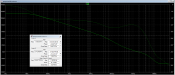
Here is OLG sim for this amp:
PM=51 degrees (very good!)
GM=7.26dB (decent but not great)
I'm still learning this stuff, so forgive if some of my info here is not right. Perhaps someone
can correct my statements if needed.
PM=51 degrees (very good!)
GM=7.26dB (decent but not great)
I'm still learning this stuff, so forgive if some of my info here is not right. Perhaps someone
can correct my statements if needed.
Attachments
Last edited:
Here are "steps for dummies" that I use:
===================================
Steps to measure GM/PM:
1) Add voltage source in the feedback loop.
DC=0V
AC=1V
Name: Vi
2) Add a node (NET label) called PROBE - between Vi and the feedback resistor.
Make sure there is a node OUT already defined for the output of the amp.
3) remove/disconnect all other AV/DC sources (e.g. input sines)
4) comment out all .tran, .ac, .four commands from your sim
5) add new ".ac dec 100 1 50meg" command
6) run sim
7) Add Trace to the plot. Expression: -1*V(OUT)/V(PROBE)
You gonna see a plot with 2 lines.
8) open a cursor window and define "cursor 1" for the point where THICKER line
crosses 0dB
9) open/create another "cursor 2" for the point where THINNER line
crosses 180 degrees
10) see the diff of values between both cursors
11) you can add this function:
.func olg() -1*V(out)/V(probe)
to the "Plot Defs File", so you can simply type "olg()" in the Expression window (step 7) instead of whole expression
LTSpice will remember this, and you can use in all your sims.
Last edited:
This thread should be split. It's no longer Latfet Amp Based on Philips AH578 and is now HEXFET Amp Based on Philips AH578 !🙂
- Home
- Amplifiers
- Solid State
- LatFet Amp Based on Philips AH578