I know, right?
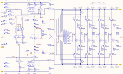
The SOA circuit has the usual number of components for 2-slope SOA limiting. Only U1A, Q1, U2A, and Q2 are additional.
The auto-bias circuit is more complicated, for certain. It replaces the Vbe multiplier and gives perfect thermal tracking output transistor bias. In a production amplifier, you would not even need to adjust a bias pot.
The amplifier itself is not that complicated, as 200W amplifiers go. After all, it only has one gain stage.
Elvee did something similar few years ago (I mean auto-biasing).
♫♪ My little cheap Circlophone© ♫♪
I built his Circlophone, and it worked really well. It didn't scale well for bigger power though...
♫♪ My little cheap Circlophone© ♫♪
I built his Circlophone, and it worked really well. It didn't scale well for bigger power though...
Elvee did something similar few years ago (I mean auto-biasing).
I am ashamed to admit that I cannot figure out how his auto-bias circuit works, but it apparently does.
Hi folks,
I have a couple of revisions to show.
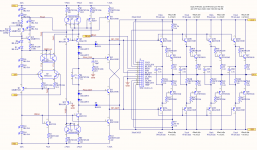
I moved the auto-bias and the SOA protection circuits to a daughter PCB, and I decided I did not want the LM334 in the bias leg. It is a bit noisy (but that would not have affected the amplifier's output noise), and it is also a PTAT, which would have increased the some of the bias current a bit at high temp. Neither of those is a big deal. In IC op amp design, we bias op amps with PTAT current on purpose, to help offset Vbe and Vgs that increase as temperature drops to -40C.
Here is the revised circuit. I also replaced the LM334 with a "ring-of-two" current source. That won't change any distortion or noise specs. I just like it better.
I have a couple of revisions to show.
I moved the auto-bias and the SOA protection circuits to a daughter PCB, and I decided I did not want the LM334 in the bias leg. It is a bit noisy (but that would not have affected the amplifier's output noise), and it is also a PTAT, which would have increased the some of the bias current a bit at high temp. Neither of those is a big deal. In IC op amp design, we bias op amps with PTAT current on purpose, to help offset Vbe and Vgs that increase as temperature drops to -40C.
Here is the revised circuit. I also replaced the LM334 with a "ring-of-two" current source. That won't change any distortion or noise specs. I just like it better.
Attachments
Very nice thread to follow, way beyond my design abilities.
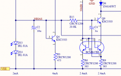
On the ring of two ccs, is a large>1M R across the bases required to guarantee startup?
Also since there is a lot of smd who or how many do you think are able to solder this up? I assume you are fine with smd but for the rest of the community it seems many are reluctant. Okay for me but for the general audience hum 🙂
Last edited:
Hi rsavas,
That is probably good advice. In a production amp, I certainly would put in a start-up resistor, so I'll add a footprint for one here.
I read the original article in Wireless World yesterday, and Peter Williams mentioned that such a thing might be necessary. He also said that all his circuits had started just fine without one, and he started them slow and with low voltage. Bob Cordell shows a 22 Meg resistor from collector to emitter of one of the transistors. That's probably a better place to put the resistor, by my circuit analysis skills.
It's a quadratic equation with two solutions, the desired bias current and zero. Leakage current and parasitics prevent zero from being a solution in the real world. Parasitic C in the transistors also provides startup current when the rails are first applied at power-up.
Thanks for the input.
Hey Russell,
Another suggestion is using a 100ohm series resistor for Q2 emitters. I know member Bonsai mention it was required in one of his amp designs to tame an oscillation.
Rick
Another suggestion is using a 100ohm series resistor for Q2 emitters. I know member Bonsai mention it was required in one of his amp designs to tame an oscillation.
Rick
I've done a lot of cascodes, and I've never seen that. Maybe the resistance on the base was too high in his circuit. Putting a resistor between the diff-pair and the cascodes is not good, in my experience.
Last edited:
I do not know of Bonsai's details, you can ask him, he is usually very forthcoming or he might chime in. I'd have to search to the thread/post, could take a long time to find.
I know Bob Cordell shows it being used too, in some schematic he showed it and other he did not for the same circuit. When I did layout on the DH-220C design, I just put them in as I guess insurance, 🙂 Bob did not complain so they stayed in.
Might be a case where the simulations do not unveil such events or it could be layout related, hard for me to say.
In the end it is your choice 🙂 You have a lot going on there.
Rick
Last edited:
I would rather put base stoppers on each individual cascode transistor, if I had an instability problem.
The distortion of the amp is fairly low, but I have not optimized it yet. There are three main sources of distortion that I see.
- The input pair. I will try increasing R2 and R4, while decreasing C11. This will increase the linearity of the input pair, especially at high frequency, but leave less feedback to correct output stage distortion at low frequency.
- Distortion from the current mirror Q7. I will try bootstrapping Q9 base to the top of R9, which should reduce distortion of the mirror. This may be the dominant distortion in the amp right now, but it is mostly 2nd harmonic. Will I be doing more harm than good to the sonics of the amp? This may also increase gain a little.
- Output stage distortion. There is not anything else I can do to cure output stage distortion. I just have to balance output stage distortion with input stage distortion, because extra emitter degeneration on the input pair will reduce the feedback that reduces output stage distortion.
Attachments
Hi Russell,
If I'm not wrong you use just simple shunt compensation, why don't try Two Pole Compensation, like my OITPC here?OITPC - Output inclusive TPC (not TMC)
I'm very interested of your opinion.
Damir
If I'm not wrong you use just simple shunt compensation, why don't try Two Pole Compensation, like my OITPC here?OITPC - Output inclusive TPC (not TMC)
I'm very interested of your opinion.
Damir
Hi Damir,
I think 2-pole output-inclusive compensation is the way to go with amplifiers that have a regular VAS stage as opposed to a folded cascode. It lets you raise the dominant pole of the amplifier to get higher loop gain at the top of the audio bandwidth, without changing the amplifier's stability. Output inclusive compensation reduces distortion of the output stage above the dominant pole, which global feedback cannot do. Furthermore, the output stage helps to charge the Miller cap, instead of the VAS, so slew rate is much higher.
I am still investigating how to do this with a folded cascode. Traditionally, folded cascode amplifiers are compensated by C to gnd at the output of the VAS. The impedance at that node is so high, that a few 10's of pF does the job nicely. I think that Miller compensation can only connect to the input, which makes it input-inclusive compensation. When I tried it, 2pF of C was the value that stabilized it. That would be great, but I'm not sure I trust just 2pF of C to compensate an amp, in the presence of other layout parasitics. One thing is certain--in layout, the output node of folded cascode stage cannot be allowed anywhere near the input nodes of the amp.
I looked at two-pole and output-inclusive about a month ago for the folded cascode, and I could not figure out how to do it. Now I am looking at it freshly, and it seems like it might be easy enough. However, I'm not sure that output inclusive feedback is any different than global feedback, if the compensation is input-inclusive.
Thanks for the comment. You may have caused me to rethink something I had given up on. I am now studying Doug Self's book, pages 336 to 349 again, and maybe seeing how to do at least two-pole compensation.
- The input pair. I will try increasing R2 and R4, while decreasing C11. This will increase the linearity of the input pair, especially at high frequency, but leave less feedback to correct output stage distortion at low frequency.
- Distortion from the current mirror Q7. I will try bootstrapping Q9 base to the top of R9, which should reduce distortion of the mirror. This may be the dominant distortion in the amp right now, but it is mostly 2nd harmonic. Will I be doing more harm than good to the sonics of the amp? This may also increase gain a little.
- Output stage distortion. There is not anything else I can do to cure output stage distortion. I just have to balance output stage distortion with input stage distortion, because extra emitter degeneration on the input pair will reduce the feedback that reduces output stage distortion.
I decided to do item 2). I bootstrapped a 1uF cap from Q9 base to the top of R9 as shown. 20 kHz isolates the bootstrapped base from the tail current node and provides an 8 Hz LF cutoff for the bootstrapping. Here's the THD comparison while driving 100W into 8 ohm:
20 Hz to about 600 Hz,
-No bootstrap: 0.45m%
-Bootstrap: 0.041m%
4 kHz
-No bootstrap: 0.56m%
-Bootstrap: 0.56m%
20 kHz
-No bootstrap: 1.6m%
-Bootstrap: 1.96m%
THD drops by about 10%, up to 600 Hz. Above 600Hz it rises more quickly than without the bootstrapping. At 4 kHz, THD is about the same with or without the bootstrap. At 20 kHz, THD with bootstrap is 20% worse.
As a sanity check, I unhooked R15 from the NBIAS node and hooked it instead to a 2.55V ideal voltage source to VEE. I wanted to be sure that C4 was not modulating the tail current. The THD result was identical.
I looked at the voltages at Q9 base and R9 emitter, and they tracked well. There is almost no current swing in the VAS stage until the frequency gets above 600 Hz. With DC current = 2.4 mA, here is the AC current swing
Freq ..... I(R9) AC pk-pk
20 Hz .... 10.5uA
200Hz ... 10.5uA
2 kHz .... 24.7uA
20kHz ... 225uA
I also tried hooking the bottom of C4 to R6 instead of R9. The THD was about 10% to 30% worse than when bootstrapped to R9. That's odd. The voltages on the tops of R6 and R9 should be nearly the same.
My conclusion is that the bootstrap of the mirror cascode base to Re of the current mirror is not desirable. It interferes with the operation of the mirror more than it helps with keeping the voltage on Q7 constant, depending on frequency. That's all for now. I'm tired.
Attachments
Lol, no. I'm a night owl.Hi Russell, do you ever sleep, so quick response from Texas?😀
Balancing RE and Ccomp
I tried increasing R2, R4. I swept these R values, while simultaneously reducing C3 (Ccomp) by the same proportion. This keeps loop gain constant above the dominant pole and keeps the amplifier stability roughly the same. For the lowest RE values, I am overcompensating with this technique.
100Hz THD (20 harmonics)
I think my new plan is to set RE to 10 or maybe 5 ohms. The SSM2212 is highly matched, so this should be plenty. I might even try no RE.
I will have to go back to Input-Inclusive Compensation. Otherwise the slew rate will drop too much. That will also let me do Two-Pole compensation, I think.
- The input pair. I will try increasing R2 and R4, while decreasing C11. This will increase the linearity of the input pair, especially at high frequency, but leave less feedback to correct output stage distortion at low frequency.
I tried increasing R2, R4. I swept these R values, while simultaneously reducing C3 (Ccomp) by the same proportion. This keeps loop gain constant above the dominant pole and keeps the amplifier stability roughly the same. For the lowest RE values, I am overcompensating with this technique.
100Hz THD (20 harmonics)
- RE ... THD m%
1 .... 0.196
5 .... 0.243
10 ... 0.303
15 ... 0.364
22 ... 0.450
33 ... 0.584
47 ... 0.754
I think my new plan is to set RE to 10 or maybe 5 ohms. The SSM2212 is highly matched, so this should be plenty. I might even try no RE.
I will have to go back to Input-Inclusive Compensation. Otherwise the slew rate will drop too much. That will also let me do Two-Pole compensation, I think.
I tried two-pole, input-inclusive compensation (TPIIC). It cannot be used by itself to stabilize the amp. Most of the original shunt C to ground from the FC output must remain.
The best improvement I could get is about 3 dB at 10kHz and 20kHz. Fundamental stability factors of the amp were compromised: PM was about the same, but GM dropped from 9 db to 6 dB, and there is a small resonance at the GM margin frequency, that I could not smooth out without losing all benefit of the TPIIC.
I believe I will stick with Cshunt at the FC output, with the higher gain due to lower RE. I will use some IIC to improve slew rate.
- The input pair. I will try increasing R2 and R4, while decreasing C11. This will increase the linearity of the input pair, especially at high frequency, but leave less feedback to correct output stage distortion at low frequency.
- Distortion from the current mirror Q7. I will try bootstrapping Q9 base to the top of R9, which should reduce distortion of the mirror. This may be the dominant distortion in the amp right now, but it is mostly 2nd harmonic. Will I be doing more harm than good to the sonics of the amp? This may also increase gain a little.
- Output stage distortion. There is not anything else I can do to cure output stage distortion. I just have to balance output stage distortion with input stage distortion, because extra emitter degeneration on the input pair will reduce the feedback that reduces output stage distortion.
I have eliminated the first and second as dominant distortion sources, leaving output stage distortion as the primary distortion. It shows up in two ways:
- Crossover distortion. I've measured this as 0.06% open loop at 20 kHz. If I can keep 40 dB of loop gain at 20 kHz, that should be corrected down to 0.0006%. More feedback is better, and 20 khz loop gain can only be helped by increasing UGBW and adding two-pole compensation.
- Non-linear loading of VAS stage by the output stage. I have not measured this, but it certainly is there. What is interesting is that when the output stages are driven by the VAS, instead of an ideal voltage source, crossover distortion seems to cancel out, somewhat. Push-pull EF stages like to be current driven, apparently.
I believe I can increase the bias of the pre-driver stage. That will reduce OL gain, but may increase the linearity of the loading by the output stage.
- Home
- Amplifiers
- Solid State
- RK-Auto200W Amplifer