my ACP+ worked from the turn on, what is going on with yours? ACP+ is very simple, it runs hot, and sounds terrific!
keep going, but unless you give us some more data, we can not help
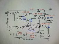
measure each important spot on the board and place the DC voltage values in the schematics, post it
ZM will be with you shortly 🙂
keep going, but unless you give us some more data, we can not help
measure each important spot on the board and place the DC voltage values in the schematics, post it
ZM will be with you shortly 🙂
you can use those testers to check functionality and pinout, not to compare electrical values with given ones in datasheet
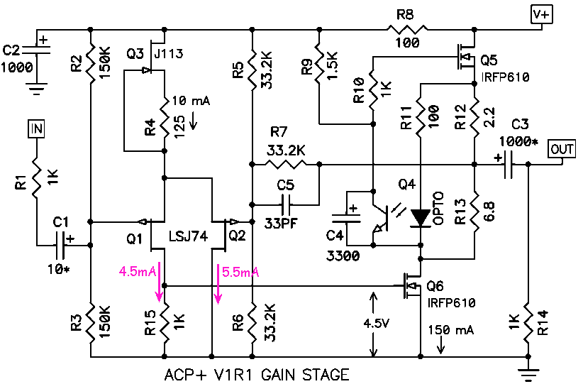
can you check voltages at important points in circuit?
drain of Q5 (ref to gnd)
voltage across any source resistor of output mosfets
voltage across R4 (ref to gnd)
voltage at Q1 gate (ref to gnd)
voltage at both sides of R7 (ref to gnd)
can you check voltages at important points in circuit?
drain of Q5 (ref to gnd)
voltage across any source resistor of output mosfets
voltage across R4 (ref to gnd)
voltage at Q1 gate (ref to gnd)
voltage at both sides of R7 (ref to gnd)
Here are the values:
drain of Q5 (ref to gnd)
L channel 0.438 R Channel 0.419
voltage across any source resistor of output mosfets
Not sure which one so I measured these
r11 L channel 0 R channel 0
r12 L channel 0.07 R channel 0.027
r13 L channel 0.22 R channel 0.083
r14 L channel 0 R channel 0.001
r8 L channel 0.437 R channel 0.415
r10 L channel 0 R channel 0
r9 L channel 0 R channel 0.001
voltage across R4 (ref to gnd)
L channel 0.503 R channel 0.477
voltage at Q1 gate (ref to gnd)
L channel 11.75 R channel 11.73
voltage at both sides of R7 (ref to gnd)
L channel 19.49 and 14.34 R channel 19.85 and 14.48
If you look closely you will see a depressed strip on one edge of the chip. Orienting the chip with the strip on the bottom, pin 1 is at the lower left corner.
http://wb5rvz.org/common/locatingPin1
Thank you, maybe I gave up too easy, but I just couldn't find anything like that in my searching.
can you just solder short between all switch pads on pcb , to exclude switch from game, for now?
you simple don't have Juice coming to circuit
you simple don't have Juice coming to circuit
yes, even if most inner one (1, as you marked) is irrelevant , according to what I can see on pics you posted earlier
just short 2 and 3 together
just short 2 and 3 together
Balanced outputs for use with ACA momoblocks
Newbie question: How do balanced outputs/ inputs work and can these be retrofitted to ACA+? I read a review of ACA used as monoblocks and they mentioned the difference with the sound using the balance configuration?
Newbie question: How do balanced outputs/ inputs work and can these be retrofitted to ACA+? I read a review of ACA used as monoblocks and they mentioned the difference with the sound using the balance configuration?
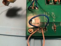
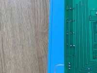
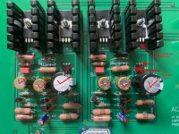
More pictures attached here. Let me know if these are okay. Thank you for taking time helping.
Attachments
-
 795B4649-914A-4525-BE9E-F9D68215899C.jpg845 KB · Views: 324
 -
 B7C16F5E-7574-4E67-BBD9-22FF503EF603.jpg919.3 KB · Views: 329
 -
 956B8888-EBFD-4439-A507-B000DE1AF54E.jpg831.1 KB · Views: 315
 -
 6FAA3967-9B88-423F-9B9F-6E0C758BB2AA.jpg751.6 KB · Views: 305
 -
 0E54E29B-57C3-40FE-BA73-A0C3D1B49711.jpg803.7 KB · Views: 321
 -
 526AB2B2-49AA-43C4-9328-874A84C7E965.jpg989.1 KB · Views: 212
to archishih #1133
Hello archishih,
Before I would exchange parts, I would reflow some solderjoints.
Especially around your Mosfets and the Optocoupler.
Reheat and add some solder.
On the pic from top I don't see the Mosfet -legs surrounded from solder?
Only some thoughts....🙄
Your caps are oriented right.
Your Optocoupler is oriented right (dot to dot).
Perhaps Mosfet N-channel Mosfet P-channel mistaken?
Greets
Dirk 😉
Attachments
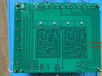
re-flow all solder joints at green power resistors, too
there must be cold solder somewhere, circuit an pcb being so straightforward
general remark - not that I didn't did same thing here and there (service job, so my mileage in this is different than regular Greedy Boy is having) but - I simply despise seeing pcb full with majority of parts augmented in size, vs. originally intended
stress which that is putting on all Vias is ridiculous, l lack of mileage resulting in not meticulously bent part wires, then increased difficulty of proper soldering of bad oriented legs in pads
recipe for disaster
and, in majority of cases , reason for oversize parts is "I read on forum that these XYZ parts are better than ZYX parts!"
best parts are those allowing that my thingie is operational
if in doubt, or you have a brilliant idea - ask thingie originator/constructor ...... don't just follow first dumba$$ on internet
ok, nuff with rant
been there, done that ........ made every imaginable audiophool mistake, and also some unimaginable, too
so, think I have some right to share bad experiences and point to bad habits
regarding #1134
Forget what I was writing about mistaken N- and P-channel Mosfet...🙄
This is ACP+, so two IRF610....
I am still getting the crown for dumbness!
Dirk in deep shame😀
Forget what I was writing about mistaken N- and P-channel Mosfet...🙄
This is ACP+, so two IRF610....
I am still getting the crown for dumbness!
Dirk in deep shame😀
Reflowed those soldering points and some more. The measurement results are the same. If I have cold joints somewhere, wouldn't I have different measurement on two channels? Both channels behave the same make me think there are something else wrong applied to both channels. Anyway, thank you all for the help. I think I may not be able to get it to work.
- Home
- Amplifiers
- Pass Labs
- Amp Camp Pre+Headphone Amp - ACP+