How the interface board works
The sheet number one includes the inputs and the power supplies.
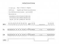
The input uses a custom PCM protocol provided by the FIFO Lite:
- data are PCM coded
- the bit frame is 32 bit per channel
- the bit clock is stopped after LRCK half cycle
- the LSB contains the sign (0=positive and 1= negative)
- bit 9, 17 and 25 are filled with zero
- bit 30, 31 and 32 are used to decode the first 2 MSBs in thermometer mode (01=001, 10=011, 11=111)
The board needs the following power supply:
- bipolar +/-3V3 to power the flip flop that manage the sign magnitude, these rails are generated dropping the +/-5V provided by the DAM1021 to +/-3V3
- single 3V3 for the rest of the board, this rail is provided by the FIFO Lite
The sheet number 2 contains the circuit to manage the conversion of the 32 bit input frame into 4 frame of 8 bit each in order to feed the 595 banks of the DAM1021.
The incoming data are simultaneously deserialized and serialized again in the new frame format. 32 bit clock allow to shift the 32 data bit along the 4 cascaded 164 shift registers until they are full filled.
In the same time the stored data are pumped out by the first output of each shift register.
Every bit clock to the four shift registers feed in parallel the inputs of the 4 x 595s contained in each bank of the DAM1021, so that in each 595 of the banks flow 32 bit instead of the allowed 8 bit.
But since each 595 is fed from a different shift register (one to one relation) finally the incoming data are correctly realigned. Each 595 discards 24 of the 32 bit flow and keeps the last 8 bit received, that are just the expected data.
For example the MSB (the first of the 32 incoming bit) crosses all the 595s but at the end it's discarded from 3 of them to be fixed only in the last register of the last LVC595 of the bank.
In the same manner the LSB (the last bit of the incoming 32 bit) is pumped out to the first register of the first LVC595 of the banks only, since it arrives with the last bit clock before it get stopped.
This way we also have the certainty that in the end the first register of the first LV164 of the interface board will contain always the sign.
The third sheet contains the output circuit of the interface board used to feed the DAC of DAM1021 replacing its original front end.
The bit clock signal to the DAM is inverted using a pair of LVC04.
This allows data to be stabilized managing the propagation delay of the logic devices in order to avoid meta stability.
Like in the original DAM the output signals are AC coupled to feed correctly both bipolar banks, the positive and the negative ones.
The bunch of 27R series resistors are used to prevent reflections from the 595s installed in the DAM to the interface board circuit, since each output signal is used to feed in parallel more than 1 input of the DAM.
A fanout buffer, the NB3L553, has been used to drive at best the LRCK, the most critical clock of the DAM.
Each output of the buffer drives one bank of the DAM with AC coupling and anti reflections series resistors.
The last sheet is the circuit used to manage the sign magnitude notation of the DAM1021.
4 flip flop have been used to sync the sign of each bank.
They are clocked with the LRCK but in this case the output of the interface board to the DAM is bipolar so the AC coupling is not needed.
Maybe the layout of the PCB will require 4 layers to avoid inappropriate interferences between the different clocks.
The sheet number one includes the inputs and the power supplies.
The input uses a custom PCM protocol provided by the FIFO Lite:
- data are PCM coded
- the bit frame is 32 bit per channel
- the bit clock is stopped after LRCK half cycle
- the LSB contains the sign (0=positive and 1= negative)
- bit 9, 17 and 25 are filled with zero
- bit 30, 31 and 32 are used to decode the first 2 MSBs in thermometer mode (01=001, 10=011, 11=111)
The board needs the following power supply:
- bipolar +/-3V3 to power the flip flop that manage the sign magnitude, these rails are generated dropping the +/-5V provided by the DAM1021 to +/-3V3
- single 3V3 for the rest of the board, this rail is provided by the FIFO Lite
The sheet number 2 contains the circuit to manage the conversion of the 32 bit input frame into 4 frame of 8 bit each in order to feed the 595 banks of the DAM1021.
The incoming data are simultaneously deserialized and serialized again in the new frame format. 32 bit clock allow to shift the 32 data bit along the 4 cascaded 164 shift registers until they are full filled.
In the same time the stored data are pumped out by the first output of each shift register.
Every bit clock to the four shift registers feed in parallel the inputs of the 4 x 595s contained in each bank of the DAM1021, so that in each 595 of the banks flow 32 bit instead of the allowed 8 bit.
But since each 595 is fed from a different shift register (one to one relation) finally the incoming data are correctly realigned. Each 595 discards 24 of the 32 bit flow and keeps the last 8 bit received, that are just the expected data.
For example the MSB (the first of the 32 incoming bit) crosses all the 595s but at the end it's discarded from 3 of them to be fixed only in the last register of the last LVC595 of the bank.
In the same manner the LSB (the last bit of the incoming 32 bit) is pumped out to the first register of the first LVC595 of the banks only, since it arrives with the last bit clock before it get stopped.
This way we also have the certainty that in the end the first register of the first LV164 of the interface board will contain always the sign.
The third sheet contains the output circuit of the interface board used to feed the DAC of DAM1021 replacing its original front end.
The bit clock signal to the DAM is inverted using a pair of LVC04.
This allows data to be stabilized managing the propagation delay of the logic devices in order to avoid meta stability.
Like in the original DAM the output signals are AC coupled to feed correctly both bipolar banks, the positive and the negative ones.
The bunch of 27R series resistors are used to prevent reflections from the 595s installed in the DAM to the interface board circuit, since each output signal is used to feed in parallel more than 1 input of the DAM.
A fanout buffer, the NB3L553, has been used to drive at best the LRCK, the most critical clock of the DAM.
Each output of the buffer drives one bank of the DAM with AC coupling and anti reflections series resistors.
The last sheet is the circuit used to manage the sign magnitude notation of the DAM1021.
4 flip flop have been used to sync the sign of each bank.
They are clocked with the LRCK but in this case the output of the interface board to the DAM is bipolar so the AC coupling is not needed.
Maybe the layout of the PCB will require 4 layers to avoid inappropriate interferences between the different clocks.
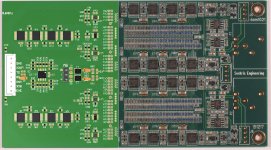
The 4 layers PCB layout of the interface board is ready.
It can be stacked on the DAM1021 using a pair of mounting holes of the original board at one side.
On the other side there are some headers to be soldered to the DAM board once 36 capacitors and 4 resistors have been removed.
The upgrade is reversible, just desolder the interface board and reinstall the original capacitors and resistors.
Attachments
The 4 layers PCB layout of the interface board is ready.
It can be stacked on the DAM1021 using a pair of mounting holes of the original board at one side.
On the other side there are some headers to be soldered to the DAM board once 36 capacitors and 4 resistors have been removed.
The upgrade is reversible, just desolder the interface board and reinstall the original capacitors and resistors.
Fast work Andrea! 🙂 What are you using for PCB layout?
TCD
Yes that was swiftly marched 🙂
How will you attach to the DAM? I see these vias, are they usable?
//
How will you attach to the DAM? I see these vias, are they usable?
//
Fast work Andrea! 🙂 What are you using for PCB layout?
TCD
Altium.
Yes that was swiftly marched 🙂
How will you attach to the DAM? I see these vias, are they usable?
//
With the pin headers at the left side of the interface board.
I have to understand if I can avoid to remove 36 capacitors and 4 resistors.
When the FPGA is not programmed its outputs go to high impedance, so I could avoid to remove capacitors and resistor since they are isolated.
But since the designer does not help I have to understand by myself how I can avoid to get the FPGA programmed at startup.
I believe the firmware is stored on the flash but I don't know how it's injected in the FPGA.
Pin headers touching the exposed pads once the caps are removed? Then soldered.
//
//
Last edited:
Yes, but I'm trying to understand if there is a way to avoid removing caps and resistors soldering directly the pin headers to caps and resistors pads at the opposite side of the FPGA.
Why not like this? Less radiation into the ladder?
//
That would also be my preferred solution.
Why not like this? Less radiation into the ladder?
//
At the beginning I thought to the way you are pointing out, but there is a problem with the height of the filter capacitors installed on the board (more than 10 mm).
I did not find any suitable pin headers with such that height (at least 12-13 mm).
Moreover this way, if I don't find a way to switch off the VCXO, the interface board would get all the radiations from the front end circuit of the DAM.
Maybe there is a simpler and less invasive way to install the interface board removing one component only.
Indeed removing the 3V3 on board LDO the VCXO, the FPGA, the micro and the flash will be no longer powered so the outputs of the FPGA will be in high impedance state that means no needs to remove 36 capacitors and 4 resistors, but simply
just solder the pin headers to one of their pads, the one connected to the 595 banks.
I could provide a little board to install in place of the LDO.
This little board will provide the footprints to reinstall the removed LDO and a dip switch to connect or disconnect the input pin of the LDO from the power rail.
This way the DAM will work in both configuration (the original DAM and the tweaked one) without any further hardware update simply connecting and disconnecting a pair of cables to the interface board and swithing on/off a dip switch.
Maybe you should investigate the option to clear the FW? All the fpga and uC files are for download. Soekris Audio ApS, Downloads But maybe you need an other tool and interface to restore this and it cold be complicated... never looked into it but someone did this operation the 1021 thread... or was in the Brewing one?
//
//
I believe that if it will work the best way is to get the DAM working in both configurations without any further hardware mods after the interface board has been installed.
I have to investigate a little since the designer "wast time with my questions".
I thought this was a diy audio forum not a LEGO audio forum, but maybe I was wrong.
I have to investigate a little since the designer "wast time with my questions".
I thought this was a diy audio forum not a LEGO audio forum, but maybe I was wrong.
Pin headers touching the exposed pads once the caps are removed? Then soldered.
//
Don't think you want to use solid pins => that would be catastrophic when jou want to unmout/desolder again. The pitch also does not match, so what you suggest is impossible (not taking into consideration having all the pins at the same length). I only see possible some thin (wire-wrap) single core wire with point to point connection => anyhow, some skills wil be needed and I would suggest not to cover the connection points on the capacitors...
Moreover this way, if I don't find a way to switch off the VCXO, the interface board would get all the radiations from the front end circuit of the DAM.
There is an RC filter to feed the VCXO: with some skills you could replace the R with a header..... just a jumper would activate/desactivate the oscillator. But I believe the filter is needed 🙂 when jou need the oscillator. A tweak is the feed the oscillator from an external supply or with a direct line from the LDO (and not use a feed-line of the FPGA)
Last edited:
That would also be my preferred solution.
You can always stick some shielding in between, the 'flying connection wires' should be as short as possible.
Don't think you want to use solid pins => that would be catastrophic when jou want to unmout/desolder again. The pitch also does not match, so what you suggest is impossible (not taking into consideration having all the pins at the same length). I only see possible some thin (wire-wrap) single core wire with point to point connection => anyhow, some skills wil be needed and I would suggest not to cover the connection points on the capacitors...
Maybe there is no need to unmount if removing the LODO will work.
However wire-wrap is a fine option.
I will provide the board without any pin connector so one can choice the preferred way.
- Home
- Source & Line
- Digital Line Level
- Implementing a true FIFO buffer with low phase noise clock on the Soekris DAM1021 DAC