If you measure at 12V you can expect they will be a little higher at 20V due to temperature coefficient
What do you mean by pads might ? on the PCB ? yes
If there is any kind of short between gate and drain of the jfet eg a solder bridge across the pads on the pcb, then they will certainly burn up
So, yes they are soldered to the PCB, but I check well after each intervention and I clean the flux.
My problem is on the -23v channel, it's the second 2SJ74 that's burning.
My problem is on the -23v channel, it's the second 2SJ74 that's burning.
Measure resistance between gate and drain.
Or measure voltage between gate and drain.
Measure voltage between gate and source.
Is it still operational or completely destroyed?
Or measure voltage between gate and drain.
Measure voltage between gate and source.
Is it still operational or completely destroyed?
Last edited:
If you are talking about R11 & R12, they are still operational (120 Ohms)
R4 heated up a lot but it still gives me 18 Ohms
R4 heated up a lot but it still gives me 18 Ohms
Last edited:
I am still talking about the jfets.
It should be virtually impossible for the jfets to burn up.
This should be the easiest issue to fix.
We will get to any other problem later.
It should be virtually impossible for the jfets to burn up.
This should be the easiest issue to fix.
We will get to any other problem later.
Ok
I placed the JFETs on a universal tester, it only recognizes them by 2 resistors of 25 Ohms G / S and G / D.
I placed the JFETs on a universal tester, it only recognizes them by 2 resistors of 25 Ohms G / S and G / D.
Good evening,
I put the JFET back in place, it continues to smoke:
- G / S 2,7v
- G / D 2,7v
- D / S 6v
I always remain septic about my rail voltage, the JFETs are sensitive (according to Mr PASS) and the TOSHIBA are given for 25v.
And I don't think my JFETs are TOSHIBA.
I measured my JFETs again, I must be around 9mA under a voltage of 25v, so we are still far from the 0.4w dissipation.
Good evening,
I put the JFET back in place, it continues to smoke:
- G / S 2,7v
- G / D 2,7v
- D / S 6v
I always remain septic about my rail voltage, the JFETs are sensitive (according to Mr PASS) and the TOSHIBA are given for 25v.
And I don't think my JFETs are TOSHIBA.
I measured my JFETs again, I must be around 9mA under a voltage of 25v, so we are still far from the 0.4w dissipation.
Out of curiosity, can you post a photo of the JFets? I vaguely recall that simple VGS is not enough but rather, the tests i've seen to confirm fakes is by charting the curves from varying voltages and current?
The Gate to Drain Measurement is bizarre
The Drain to source measurement is impossible, unless voltage at source is well above 0V potential.
The Drain to source measurement is impossible, unless voltage at source is well above 0V potential.
Hello,
here are the values measured on the PCB:
(I added the polarity, knowing that the negative of the voltmeter is placed on the Gate and the 0v.)
- G / S + 2,9v
- G / D - 2,9v
- 0v / S - 18,5v
- 0v / D - 24,5v
It is also useful to point out that the trimpots are at their lowest.
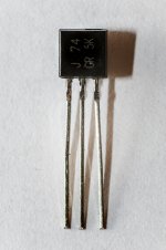
@ Super BQ: attached the photo of a JFET
On the photo it's GR, but I also have BL, the case is identical and the typography too.
here are the values measured on the PCB:
(I added the polarity, knowing that the negative of the voltmeter is placed on the Gate and the 0v.)
- G / S + 2,9v
- G / D - 2,9v
- 0v / S - 18,5v
- 0v / D - 24,5v
It is also useful to point out that the trimpots are at their lowest.
@ Super BQ: attached the photo of a JFET
On the photo it's GR, but I also have BL, the case is identical and the typography too.
Attachments
Last edited:
I think, this JFETS are not "B" Grade.. and honestly, they don't look to be genuine..
I bought genuine Toshiba's from ebay seller punkydawgs (smbd here recommended this seller).
Toshiba 2SJ74 + 2SK170 LAB MATCH QUAD to 0.03mA & 4mV (9-10mA range "BL" "B") | eBay
I bought genuine Toshiba's from ebay seller punkydawgs (smbd here recommended this seller).
Toshiba 2SJ74 + 2SK170 LAB MATCH QUAD to 0.03mA & 4mV (9-10mA range "BL" "B") | eBay
Yes I have already ordered from this seller, but more than a month to be delivered 🙁
There is also Alweit in Israel, I will contact him.
I must first solve this problem before putting a good JFET.
There is also Alweit in Israel, I will contact him.
I must first solve this problem before putting a good JFET.
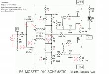
I eliminate step by step to see where this tension comes from.
I started by rectifying the DC voltage with the Trimpot OFFSET, then I separated the positive circuit by removing the 2SK170 first, then R4 and R1.
View the photo
Quel serait la suite logique selon vous ?
I started by rectifying the DC voltage with the Trimpot OFFSET, then I separated the positive circuit by removing the 2SK170 first, then R4 and R1.
View the photo
Quel serait la suite logique selon vous ?
Attachments
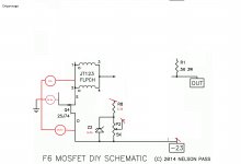
Continued my inspection, removed the IRFPs, removed all the links that could raise a voltage at the terminal of OUT, NOKAnglais
The JFET must be totally HS, disassemble the JFET, replace with another, I get:
0v / D -26.4v normal
0v / G -14.6v
0v / S -25v
Here is what remains of the circuit and always this tension.
The JFET must be totally HS, disassemble the JFET, replace with another, I get:
0v / D -26.4v normal
0v / G -14.6v
0v / S -25v
Here is what remains of the circuit and always this tension.
Attachments
- Home
- Amplifiers
- Pass Labs
- F6 Illustrated Build Guide