Someone can help me: P3-LogicPower board will be lead to P3-uC board (6V) and P2-Preamp board (5V)? Is P3 missing from uC BOM?
I would tell you a lie if I told you I only understood one thing in your sentence 😱
I would tell you a lie if I told you I only understood one thing in your sentence 😱
Sorry for my English. I would like to know where pin P3 of LogicPSU board connected to?
Hi gionag 🙂
I don't think you are missing a BIG point !
I think like you do : Why increase the gain in front of the Muses ? Most of the sources have an output of 2v p/p (or more), like CD-players, Dac's and so on.
I use my pre. with the gain stage AFTER the Muse's, and no buffer.
I'm sure you will gett better thd. readings in this way.
But let's see Alex comment on this one 🙂
Regards
Johnny
I confirm what Johnny is writing here and you are not missing anything.
There was a couple of trials done years ago when this project was under design and I agree that in the end the gain stage is better after the muse.
On my side I am using the exact same configuration as Johnny and the buffer is just shorted.
It is there just for matching impedance purpose but not mandatory, anyway his distortion level is really low so it does not hurt.
Then regarding the matching of the real measured attenuation vs. the displayed one, I made some measurements this morning again to re-check.
So the UGS v3 with the default resistor implementation as on the UGS v3 schematics produces on my side a gain of ~3.17dB in unbalanced mode.
Before I was considering the theoretical value of 4.4dB (unbalanced) / 10.4dB (balanced) but it is a bit less as I measured.
So I adjusted the software to have a displayed level a bit more accurate to the real one attenuated by the muse.
I believe the -3dB you see should be in unbalanced mode correct? With the new FW it should be less, you should have close to 0dB if your UGS gain is similar to mine.
Last to explain what the menu configuration of the UGS module does, when set to others, what is displayed exactly matches the muse attenuation in the datasheet, when set to UGS I am adding an offset to compensate the UGS V3 gain (basically 3dB here in unbalanced).
Balanced value cannot be measured straight forward on my side, so I will do this later on and adjust as I need to connect a balanced source to the preamp.
Last edited:
While we are waiting...
someone has already measured the output voltage that comes from the TPS7A4901 and the TPS7A3001 (+/-vdda)?
I am asking because mines reports values quite different from each other.
having 4 rails in total (+/- on the left and right) values ranges from 16.0 and 16.8 volts. input voltage is > 20.
Just to be clear, voltage on each rails is stable as a rock, both loaded and unloaded. is an absolute different between each of them.
i have seen the values for the feedback network of the regulatos (voltage set) in schematic are different from the one in BOM.
Values in BOM are much higher values than then one reported in schematics.
I have checked with the datasheets, and the ratio match, so the voltage in the end should be the same, but a think that concerns me a little is the minimum current that datasheet requires in the feedback network in order to be accurate and stable... the datasheet report a minimum current of 2.5ua, with "schematic" values, that should be ~1ma (plenty) and the one in the bom led to 5ua (double the minimum, but still few order of magnitude less than the one reported in schematic).
Some clarification would be much appreciated.
I would swap values right away, but i am used to think that if something doesn't match, usually, its me missing some important technical aspect, rather than others mistake (oversights...)
Thanks
I did not recall about this immediately (as this design was done in 2013...) so I checked my PCB and indeed the value I have mounted are larger than the one on the schematics.
What I remember well on the other hand is that I destroyed at that time 2 or 3 TPS7Axxxx LDO when debugging, plugging / unplugging power.
This is why later on I added the protections diodes and resistor to limit the inrush current and then I did not break anymore a LDO.
Probably the resistor divider was modified at that time too and not updated on the schematics (sorry about that...)
Anyway you are free to adjust the divider network to lower resistor values and make some tests.
I measured the voltage rails on my L/R preamp board and they are similar for the same LDO (because there is a small delta between the positive and negative one).
Sorry for my English. I would like to know where pin P3 of LogicPSU board connected to?
Hello,
The connector P3 pin 3&4 of the logic power board is connected to the connector P3 pin 1&2 of the control board
schematic have been posted by Eric earlier in this postSorry for my English. I would like to know where pin P3 of LogicPSU board connected to?
Attachments
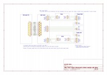
Thank Eric and Hicoco. I ask because I don't see P3 in uC BOM. But it is clear for me now.
Best regards,
Bruce Lee
Best regards,
Bruce Lee
I confirm what Johnny is writing here and you are not missing anything.
There was a couple of trials done years ago when this project was under design and I agree that in the end the gain stage is better after the muse.
On my side I am using the exact same configuration as Johnny and the buffer is just shorted.
It is there just for matching impedance purpose but not mandatory, anyway his distortion level is really low so it does not hurt.
Then regarding the matching of the real measured attenuation vs. the displayed one, I made some measurements this morning again to re-check.
So the UGS v3 with the default resistor implementation as on the UGS v3 schematics produces on my side a gain of ~3.17dB in unbalanced mode.
Before I was considering the theoretical value of 4.4dB (unbalanced) / 10.4dB (balanced) but it is a bit less as I measured.
So I adjusted the software to have a displayed level a bit more accurate to the real one attenuated by the muse.
I believe the -3dB you see should be in unbalanced mode correct? With the new FW it should be less, you should have close to 0dB if your UGS gain is similar to mine.
Last to explain what the menu configuration of the UGS module does, when set to others, what is displayed exactly matches the muse attenuation in the datasheet, when set to UGS I am adding an offset to compensate the UGS V3 gain (basically 3dB here in unbalanced).
Balanced value cannot be measured straight forward on my side, so I will do this later on and adjust as I need to connect a balanced source to the preamp.
Ok, just to be clear, both of you mount a ugs gain stage after the MUSE (M1 position) without buffer on M2. that's right ?
or maybe you are using also the buffer on M2 (after the gain->muse chain) ?
simulations reports the same theoretical value you assumed:
▶ with single-ended input
~4.4db on single-ended output
~10.4db on differential output
▶ with differential input we should have
~10.4db on single ended output
~16.4db on differential output
Said that, as i already measured, can be easily a little under that. and hence the 0.7 V/V gain i see at 0db. instead of 1 V/V (or close to that).
I am pretty sure i have the input configured as balanced, but later i will check also that.
The tweak you already did to the FW is a good improvment... but, if is not an huge work, can be very nice to add an offset adjustment for the volume control. So each of us can tune the scale for their own needs. for example, jhonny uses an UGSv6 that i must assume play with different gain values, and i think could be nice to account for this variable.
Later i will measure my UGSv3's (both with unbal and bal input) and report real values, just to have more data to check against.
Thanks (as always...)
I did not recall about this immediately (as this design was done in 2013...) so I checked my PCB and indeed the value I have mounted are larger than the one on the schematics.
What I remember well on the other hand is that I destroyed at that time 2 or 3 TPS7Axxxx LDO when debugging, plugging / unplugging power.
This is why later on I added the protections diodes and resistor to limit the inrush current and then I did not break anymore a LDO.
Probably the resistor divider was modified at that time too and not updated on the schematics (sorry about that...)
Anyway you are free to adjust the divider network to lower resistor values and make some tests.
I measured the voltage rails on my L/R preamp board and they are similar for the same LDO (because there is a small delta between the positive and negative one).
Ok, first thing first
you are confirming that with values of 47k5 and 604k (as per BOM and also the ones you currently have on your preamp) values on the positive rails and slightly different from the one on the negative, I understood correct ?
But, you also saying that positives and negatives between L and R are consistent between themselves...
I have not fitted the protection components (diode and resistors), but rather placed two 0-ohm jumper in theirs places
Done that because i am fitting shunt regulators before and they are intrinsically current limited.
i will try with values that allow's more current to be flown in the fb network itself and see if that closes the gap between the values.
In the end, a nice smd, lowppm trimmer can be fitted to align each rail to each other.
i don't think that is a mandatory requirement, but i am still trying to understand if we are riding some sort of edge case or is all normal.
What do you think about that ?
Thanks (again...)
the datasheet report a minimum current of 2.5ua, with "schematic" values, that should be ~1ma (plenty) and the one in the bom led to 5ua (double the minimum, but still few order of magnitude less than the one reported in schematic).
must correct this part... was 25uA ... not 5uA.
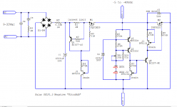
UGSv3 in-circuit measurements
For whom interested,
with the UGSv3 with 24v supply. Rg/Rfb/Rin as per BOM.
2sk389BL / 2sj109BL + ZTX450/550.
from simulation we should have :
▶ ~ 4.4 dB of gain when inputs are wired as SINGLE-ENDED (UNBAL)
▶ ~ 10.4 dB of gain when inputs are wired as DIFFERENTIAL (BAL)
from my measurements:
▶ ~ 3.9 dB of gain when inputs are wired as SINGLE-ENDED (UNBAL)
▶ ~ 9.9 dB of gain when inputs are wired as DIFFERENTIAL (BAL)
values was taken from the output as gnd referenced (single-ended). in differential the output is +6db (as per theory), this was also checked and matched on the real module.
this might help to re-adjust the volume scale (if the option to let user decided is discarded, otherwise, every and each of us can tare the system according to their needs, module configuration)
Hope this helps.
Last edited:
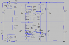
Shunt board negative rail issue.
I have a problem....
I built Eric's new PSU and shunt boards. I've been testing one of the boards - under load - and been able to adjust the + rail to the correct 24VDC. However on the - rail, I'm only able to adjust the trimmer to a max of -14VDC.
At first, I was only getting -5VDC on the - rail, so I replaced Q108 and that brought it up to -14VDC. However, now I'm stumped, and wondering what part may be bad. I have replacement parts for everything if someone more knowledgeable than me could guide me where to focus.
First check if the current in the CCS jfet are right. if they are low you can't adjust the output voltage correctly.
redjr you should read this https://www.diyaudio.com/forums/pow...ultrabib-shunt-regulator-156.html#post5830413I have a problem....
I built Eric's new PSU and shunt boards. I've been testing one of the boards - under load - and been able to adjust the + rail to the correct 24VDC. However on the - rail, I'm only able to adjust the trimmer to a max of -14VDC.
At first, I was only getting -5VDC on the - rail, so I replaced Q108 and that brought it up to -14VDC. However, now I'm stumped, and wondering what part may be bad. I have replacement parts for everything if someone more knowledgeable than me could guide me where to focus.
R4>>R105
R7>>R110
R8>>R112
you can measure the voltage drop across each one's source resistor and divide by its Ohmic value. You should have <= 2,7V for 270R value
Ok, first thing first
you are confirming that with values of 47k5 and 604k (as per BOM and also the ones you currently have on your preamp) values on the positive rails and slightly different from the one on the negative, I understood correct ?
But, you also saying that positives and negatives between L and R are consistent between themselves...
I have not fitted the protection components (diode and resistors), but rather placed two 0-ohm jumper in theirs places
Done that because i am fitting shunt regulators before and they are intrinsically current limited.
i will try with values that allow's more current to be flown in the fb network itself and see if that closes the gap between the values.
In the end, a nice smd, lowppm trimmer can be fitted to align each rail to each other.
i don't think that is a mandatory requirement, but i am still trying to understand if we are riding some sort of edge case or is all normal.
What do you think about that ?
Thanks (again...)
Actually I don't have exactly the same (don't ask me why because this is long time ago...), as I can read 51.1K on one and nothing on the other one as there is no silkscreen marking on it and measuring it on-board gives a very large value which mean I have to unsolder it to understand, which I did not do.
My muse rails are lower than yours, around 15V that explains probably why I have 51.1K rather than 47K.
Anyway once again you are free to adjust the R couple the way you want and reduce values to drain more current.
Then I just looked again at the TPS7A49 datasheet for example and the overall output accuracy is +/-2.5% which gives +/-400mV for a 16V rail...
That is maybe one of the reason, TI explains later on to use 0.1% R and take into account the output voltage offset to get an accurate output.
In my opinion, it is not important to have an accurate output as long as the voltage are fixed which you confirm is what you see.
Be careful removing protections those LDO hate reversed current.
I have a problem....
I built Eric's new PSU and shunt boards. I've been testing one of the boards - under load - and been able to adjust the + rail to the correct 24VDC. However on the - rail, I'm only able to adjust the trimmer to a max of -14VDC.
At first, I was only getting -5VDC on the - rail, so I replaced Q108 and that brought it up to -14VDC. However, now I'm stumped, and wondering what part may be bad. I have replacement parts for everything if someone more knowledgeable than me could guide me where to focus.
Verify Q104 that E and C pins are not shorted together since my simulations shows approximately the same voltage that you measure if I do so.
In case here are the simulated measurements points for +/- 24V outputs.
Attachments
redjr you should read this https://www.diyaudio.com/forums/pow...ultrabib-shunt-regulator-156.html#post5830413
R4>>R105
R7>>R110
R8>>R112
you can measure the voltage drop across each one's source resistor and divide by its Ohmic value. You should have <= 2,7V for 270R value
On the positive rail I get;
R4 = 263mV
R7 = 600mV
R8 = 605mV
On the negative rail I get; (where the problem is)
R105 = 266mV
R110 = 247mV
R112 = 232mV
Haven't had a chance to peruse the Salas thread yet, but will.
- Home
- Amplifiers
- Pass Labs
- UGS-muse preamp GB