yes but the point is regarding passive IV increasing the sensitivity to supply quality compared to active IV, whether this is a trait of passive IV with CC dacs or any current output DAC.
I don't thing it has something to do with a passive I/V, because active I/V can provide much lower impedance (and load) than a passive resistor (unless 10R or so was used).
Last edited:
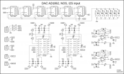
Yes, C31/C36 and R8/R9 are vacant.
Perfect! I’ll increase R4 to 2K4. Curious about if/how the sound changed? Must wait until morning to get some listening done......😀
Of course Vunce, we are waiting for your result from detailed comparison with opamps 😀
AD844 can be experimented with this pcb. Only thing to do is 'not populating i/v components and soldering 1.5k&1nf cap from pin5 to ground', using ad844's internal buffer from pin6.
Output offset can be easily trimmed with 20k across pin1,7,8. if its necessary..
Anybody tried that?
Output offset can be easily trimmed with 20k across pin1,7,8. if its necessary..
Anybody tried that?
Unfortunately, I do not have good news to report 🙁
I’m getting background hiss from the speakers that can be heard from 4 feet away, no hum. Possible oscillation? DC offset is very high 100-120mV. With music playing there is audible distortion. When R4 was increased to 2K4, there was no increase in volume output.
I checked and double checked for errors with my implementation of the OPA860 circuit, it’s good, No shorts or solder bridges.
I will try a different location for R4 &C1 GND point. Currently they are tied into the vacant C37/C38 ground pads.
Attachments

Not sure what you mean, like the lower impedance load puts more strain on power supply?I don't thing it has something to do with a passive I/V, because active I/V can provide much lower impedance (and load) than a passive resistor (unless 10R or so was used).
The dac output is current limited so I dont think it makes a difference.
Unfortunately, I do not have good news to report 🙁
...
it's a pity, maybe there will be some hidden mistake 😀 the connection is identical to that from Pedja ... at least you tried 😉
I Reinstalled the first dac board that is unmodified and have the BursonV6 opamps installed. My spirits have been lifted again!! The combo sounds fantastic 😀
I haven’t given up yet though, I will try to bypass the onboard OPA860 buffer, essentially making it an OPA861. (Those are also on the way 😉)
I haven’t given up yet though, I will try to bypass the onboard OPA860 buffer, essentially making it an OPA861. (Those are also on the way 😉)
Hm.. I can confirm that OPA861 (both..) in the circuit of Pedja (as told, I am having the Aya dac) is perfectly functional, zero instability. And sounds very good..
But, OPA861 IS a high speed circuit and care should be taken
"The 860 does get hot." - - A tale telling sign..
"The 860 does get hot." - - A tale telling sign..
Last edited:
But, OPA861 IS a high speed circuit and care should be taken
"The 860 does get hot." - - A tale telling sign..
That is also what I thought.
I do not doubt that this circuit works very well, it comes from a very respected designer. I would build it as a standalone circuit, but the BF245A transistors are obsolete, is there a suitable replacement?
Wait.. You don't need that part.. Ad1862 has it's output already biased for zero offset?!
Pedja circuit is prepared for the 1541, where pre-bias is not used..
Pedja circuit is prepared for the 1541, where pre-bias is not used..
Vunce, I had a look at your schematic.
Place a 'base stopper' resistor between the two sections if OPA860, right on the input of the output buffer. After the filter cap! Like 1kohm..
Place a 'base stopper' resistor between the two sections if OPA860, right on the input of the output buffer. After the filter cap! Like 1kohm..
Also, the input stage base would need some hundred ohm (called Rs in the data sheet). (if You look carefully, the datasheet prescribes these 'damping' resistors at both places (Rs - 20ohm-250ohm), at the OTA input stage base; at the input of the buffer stage.
Ciao, George
Ciao, George
Then, try to place a small smd ~10nF (or 100nF or between) directly on top of the smd chip, between - Vee and +Vcc (+_5Vpins, pin7, pin4).
All these things are needed, in reality, to maintain good stability..
Ciao, G
All these things are needed, in reality, to maintain good stability..
Ciao, G
Hm.. I can confirm that OPA861 (both..) in the circuit of Pedja (as told, I am having the Aya dac) is perfectly functional, zero instability. And sounds very good..
Yup ! Despite no decoupling at its feets, the magic of a good power supply design -the 100 uF caps are strategical there I mix both 47 uF & 100 uF, so a litlled isymetry, lol- Nore I use the 1500 uF Pan FM btw.
Then, try to place a small smd ~10nF (or 100nF or between) directly on top of the smd chip, between - Vee and +Vcc (+_5Vpins, pin7, pin4).
All these things are needed, in reality, to maintain good stability..
Ciao, G
Sure, as I questionned : those chips lives bad to be on a socket, on adaptaor, should be directly soldererd and careffully decoupled right at their power leads.
750 ohms is ok after the opa861, it's what I use on the AYA before the buffer..., still the opa861 reversed in mine but a better buffer should exist... though the opa861 reversed is neutral fr my tastes. Ok off topic, perhaps can give some thoughts for Vunce.
Edit : are the pins of the opa861 copatible with most opa in a swap operation ??? Not sure it is iirc! Vunce, did you populate the miro's pcb or hacked the outputt with a wire on an extra board and managed a ground between the two boards ? Or I'm not understanding you are talking about the verroboard ?
Last edited:
- Home
- Source & Line
- Digital Line Level
- DAC AD1862: Almost THT, I2S input, NOS, R-2R