Is it underbiased?
In fact it was underbiased, 16mV across 0.22R emitter resistors (70mA per output pair), but it has nothing to do with biasing.
There is no classic NFB loop but EC loop instead. (it's a buffer, voltage gain 1)
It is possible that I made a mistake when measuring. The probe was hooked up on the output transistor's emitter and the loop was big. Sadly, I forgot to add test points to the pcb. I'll make new measurements.
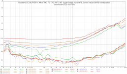
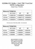
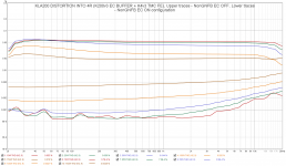
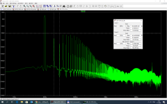
sound card measurements of the buffer K200v3
distortion NULL was set at conditions : 1kHz sine, 50W into 4R5
graphs : freq vs thd, load 4R5, power levels: 50W,100W,150W (rated power 200W/4R)
RED trace - EC loop inactive (open loop)
YELLOW trace - EC loop active


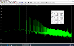
distortion NULL was set at conditions : 1kHz sine, 50W into 4R5
graphs : freq vs thd, load 4R5, power levels: 50W,100W,150W (rated power 200W/4R)
RED trace - EC loop inactive (open loop)
YELLOW trace - EC loop active


I own a precise measuring system for some time based on notch filter and sound card. I can easily measure down to -140dB.
However, measuring power amplifier under -120dB is a challenge. Everything counts, cables, connectors, dummy load. The latter two have great impact on H3/H5, higher frequencies worsen things. Just a little dirt or not perfect contact and H3 is 10db higher.
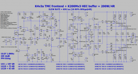
K200Mv3 EC buffer enclosed into global NFB with K4v3 TMC frontend has extreme low distortion in the simulator, THD -160dB for 1-150W/4R/1k.
I was curious how simulation differs from reality and how overall design influences the performance. The feedback path which encloses the buffer and the frontend is quite long, 18cm (two separate PCBs), so not ideal at all. I'm sure, this is one of the thing what degraded the system performance.

Pic1 - LTSpice simulation
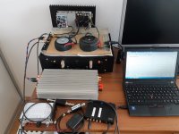
Pic2 - amplifier and measurement system on the bench
Pic3 - measurement done by ESI Julia itself (no notch filter)
Pic4 - measurement result with notch filter
However, measuring power amplifier under -120dB is a challenge. Everything counts, cables, connectors, dummy load. The latter two have great impact on H3/H5, higher frequencies worsen things. Just a little dirt or not perfect contact and H3 is 10db higher.
K200Mv3 EC buffer enclosed into global NFB with K4v3 TMC frontend has extreme low distortion in the simulator, THD -160dB for 1-150W/4R/1k.
I was curious how simulation differs from reality and how overall design influences the performance. The feedback path which encloses the buffer and the frontend is quite long, 18cm (two separate PCBs), so not ideal at all. I'm sure, this is one of the thing what degraded the system performance.
Pic1 - LTSpice simulation
Pic2 - amplifier and measurement system on the bench
Pic3 - measurement done by ESI Julia itself (no notch filter)
Pic4 - measurement result with notch filter
Attachments

Hi LKA,
Impressive work!!! Can’t believe I missed this first time round.
Going to try and apply this error correction to my “lunchtime amplifier v2” output stage. It looks as though it could be a good fit for Bob Cordell’s thermaltrak feedback bias output stage.
Best wishes,
Paul
Impressive work!!! Can’t believe I missed this first time round.
Going to try and apply this error correction to my “lunchtime amplifier v2” output stage. It looks as though it could be a good fit for Bob Cordell’s thermaltrak feedback bias output stage.
Best wishes,
Paul
Yeah, but distortion numbers don't tell how it sounds.
I listen to the bipolar non-gnfb version. HEC buffer keeps the bjt ops distortion low and the open loop frontend adds significant H2 and H3. IMHO perfect combination.
KLA200 - 200W/4R AMPLIFIER - Google Photos
Of course, HEC applied to the bjt OPS is perfect too.
K200v3 - Bipolar class AB power buffer with Hawksford Error Correction HEC - Google Photos
🙂
Last edited:
Hi LKA,,
With great respect have I followed your journey through various combinations and topologies, just because I also followed the same route of splitting the amplifier and output buffer with very satisfactory results.
I just wanted to put the HEC distortion reduction somewhat in perspective.
There is of course absolutely nothing wrong with the theory behind, but it is not that simple to realise as you must have noticed yourself, because adders and subtractors cannot be made that simple with just a few resistors plus transistors.
When looking at input minus output signal for a Hec buffer, a very distorted signal may become visible, that now became part of the output signal.
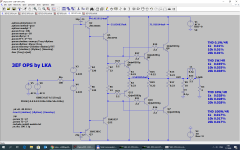
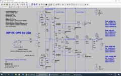
As an example I have shown below the Hec Buffer that you called "3EF EC OPS LKA" compared to exactly the same buffer without HEC.
Although the difference between input and output is larger with the Non Hec Buffer, the difference products are much less benign in the latter case, thus resulting at the end in a lower distortion.
This is for a 10Khz input signal, but the result is the same for 1kHz.
I have used a 10K Ohm source, a value that comes closer to a VAS output, but when using 100R or lower, distortion will become somewhat smaller for both versions.
I know that with your K200V3a, a four stage output buffer, you have pushed the limits again a bit further, but this posting was just meant not to look just at distortion figures, but also at the nature of the distortion, that may be worse as expected from the THD figures.
Hans
P.S. Look at H3, it is 15dB higher for the Hec version.
With great respect have I followed your journey through various combinations and topologies, just because I also followed the same route of splitting the amplifier and output buffer with very satisfactory results.
I just wanted to put the HEC distortion reduction somewhat in perspective.
There is of course absolutely nothing wrong with the theory behind, but it is not that simple to realise as you must have noticed yourself, because adders and subtractors cannot be made that simple with just a few resistors plus transistors.
When looking at input minus output signal for a Hec buffer, a very distorted signal may become visible, that now became part of the output signal.
As an example I have shown below the Hec Buffer that you called "3EF EC OPS LKA" compared to exactly the same buffer without HEC.
Although the difference between input and output is larger with the Non Hec Buffer, the difference products are much less benign in the latter case, thus resulting at the end in a lower distortion.
This is for a 10Khz input signal, but the result is the same for 1kHz.
I have used a 10K Ohm source, a value that comes closer to a VAS output, but when using 100R or lower, distortion will become somewhat smaller for both versions.
I know that with your K200V3a, a four stage output buffer, you have pushed the limits again a bit further, but this posting was just meant not to look just at distortion figures, but also at the nature of the distortion, that may be worse as expected from the THD figures.
Hans
P.S. Look at H3, it is 15dB higher for the Hec version.
Attachments

Last edited:
Hi Hans, this kind of EC needs low impedance drive because impedance is added to the 310R (through Q1, divided by beta) and can upset the EC balance. For 10k impedance try to lower R1 (cc 220R and adjust V1,V2 too) or use input buffer as I did here (mosfet version) K71 - MOSFET POWER BUFFER with ERROR CORRECTION - Google Photos
D1should be doubled for better performance.
D1should be doubled for better performance.
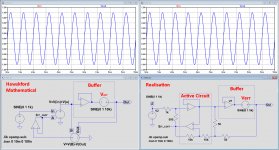
To further show what a complex task the active circuitry has to do in a Hec Buffer, I have shown in the image below at the left the mathematical model that Hawskford designed.
The model is fed with a 1Volt 1kHz input signal and and a simulated Amp error of 1Volt 5Khz.
In the time signal there is no trace of the 5Khz. it's completely eliminated.
At the right I have shown an example of a realisation, where the adders in the mathematical model are replaced by resistors, in this case 50R+50R around the Buffer and 1K and 500R at the input.
Within the striped box, the active circuitry is visible to perform all necessary functions.
Quite obvious that this is a complex task to perform for a few transistors.
It's also clear that the own distortion produced from this active circuitry is not compensated by the error correction topology.
Again a 1Khz at the input and a 5Khz Error signal is used, but also in this case there is no sign of the 5Khz.
Hans
Attachments
Hi Hans, this kind of EC needs low impedance drive because impedance is added to the 310R (through Q1, divided by beta) and can upset the EC balance. For 10k impedance try to lower R1 (cc 220R and adjust V1,V2 too) or use input buffer as I did here (mosfet version) K71 - MOSFET POWER BUFFER with ERROR CORRECTION - Google Photos
D1should be doubled for better performance.
Hi LKA,
As I mentioned in my previous posting, when driving from a low source impedance source, in this case 1R, the Hec version drops to 0.026%, corresponding with your data, and the straight buffer goes to 0.013%.
But much more important, with 1R source the Hec version has its H3 at -71dB, while the straight buffer has H3 at -89dB.
H2 is rather harmless, but H3 is not at all.
So in this case the straight buffer is the clear winner, driven from 10k as well as from 1R.
This must be a wake up call for some, at least is was for me.
So I agree what you mentioned before, listening should always be a proof of the pudding.
Hans
Btw, above is not HEC (Hawksford EC), K200 is a HEC implementation. Basically it is a 3EF preceded by a buffer stage. I compared the distortion profile with and without EC. Distortion reduction at low powers (up to 50W/4R) is significant.
Attachments
Hi Hans. As you are dealing with op amp version of Hec, can try my way , upon LKA's 3×EF ? described here Simple high power BJT/MOSFET G=0.6db output with Hawksford error corrector .
bellow is Spice model of ultra low distortion/noise CFA opamp.
My simulator is Tina , measurments are different hence uncomparable.
Hayk
bellow is Spice model of ultra low distortion/noise CFA opamp.
My simulator is Tina , measurments are different hence uncomparable.
Hayk
Attachments
Last edited:
LKA, what are the brand and part numbers of the wire connectors on your great PCB's, the ones you show are of many different colors and are seemly stack-able. Great looking boards and circuits. Thanks
Hi LKA,
As I mentioned in my previous posting, when driving from a low source impedance source, in this case 1R, the Hec version drops to 0.026%, corresponding with your data, and the straight buffer goes to 0.013%.
But much more important, with 1R source the Hec version has its H3 at -71dB, while the straight buffer has H3 at -89dB.
H2 is rather harmless, but H3 is not at all.
So in this case the straight buffer is the clear winner, driven from 10k as well as from 1R.
This must be a wake up call for some, at least is was for me.
So I agree what you mentioned before, listening should always be a proof of the pudding.
Hans
Hans, in my simulations the winner is the EC OPS (up to 50W/4R)
H2 was reduced significantly.
H3 was reduced too, not so much as H2.
I set the idle currents of the two OPS identicaly.
predriver = 6.5mA
driver = 32mA
output = 70mA per pair
Example, 10W/4R/10kHz
3EF OPS
H1 +16dB
H2 -59dB
H3 -61dB
3EF EC OPS
H1 +16dB
H2 -87dB
H3 -70dB
Attachments
Last edited:
I simulated the ec version, for 30Vp 10khz I have 0.02%.If I apply a 1T inductor in seie with the feedback 1k, I get 0.0237% . This is for 8 ohm load. With 4 ohms , with inductor is 0.187% without , 0.11%. Indeed the ec is making worse for 4 ohms.
Last edited:
To further show what a complex task the active circuitry has to do in a Hec Buffer, I have shown in the image below at the left the mathematical model that Hawskford designed.
The model is fed with a 1Volt 1kHz input signal and and a simulated Amp error of 1Volt 5Khz.
In the time signal there is no trace of the 5Khz. it's completely eliminated.
At the right I have shown an example of a realisation, where the adders in the mathematical model are replaced by resistors, in this case 50R+50R around the Buffer and 1K and 500R at the input.
Within the striped box, the active circuitry is visible to perform all necessary functions.
Quite obvious that this is a complex task to perform for a few transistors.
It's also clear that the own distortion produced from this active circuitry is not compensated by the error correction topology.
Again a 1Khz at the input and a 5Khz Error signal is used, but also in this case there is no sign of the 5Khz.
Hans
Hans, if the remaining distortion is low, of course you see no sign of it in the Vin, Vout curves.
The best way to look at this is to plot Vout-Vin. How does it look then?
Jan
- Home
- Amplifiers
- Solid State
- HEC amp