Thanks a lot for your advice, I have done something a bit like that, I have looked for other members version of the Mooly amplifier. About other amplifier designs, I did thought that it would be a bad idea to look at other amplifier designs, because I thought it could confuse more then help. But I'll 100% follow your advice and search google thin🙂
I know I may not express it in any good manner, but know that every answer I get, make me super happy!! Without your all, I have never been able to start this fantastic journey!
I know I may not express it in any good manner, but know that every answer I get, make me super happy!! Without your all, I have never been able to start this fantastic journey!
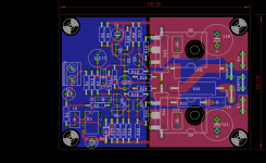
Lets take a look at prasi's fantastic design, it's beautiful!!
Unfortunately am I looking at that design with several noob questions.
prasi do use 4 mosfets (in parallel for higher current capability), these mosfets is flat against the pcb, what about heat?
I can't locate the inductor?
If I try to copy most of that fantastic design, is there things I have to be careful of, mandatory rules?
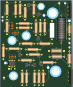
I had some trouble sleeping yesterday so...
Not really tidied up and optimized but just another example, to show how to better make use of your two layers and maximize copper use.
The mosfet go "under" the pcb, in between the pcb and the heatsink, the leads bent upwards and the whole pcb is attached to the heatsink.
Not really tidied up and optimized but just another example, to show how to better make use of your two layers and maximize copper use.
The mosfet go "under" the pcb, in between the pcb and the heatsink, the leads bent upwards and the whole pcb is attached to the heatsink.
Attachments
Hi FM,
I've also just started out in the world of PCB layouts and it can be daunting to get started, but so rewarding when you finally get to hit the 'send to production' button at the fab house website.
I use EasyEDA (which is free) and have found it simple enough to pick up fast. It isn't perfect but it does what I need. I have my second PCB in production right now - the first one, although fully functional, had a few layout characteristics that I wanted to correct.
I have a few tips that I learnt that I'd like to share:
Use the autorouter to get a sense of what should fit where - but pull everything off and lay out manually. Auto-router won't always make the most sensible choice, but can be helpful. I lock most of a layout and then auto-route to get ideas if I get stuck.
Separate your schematic into blocks - PSU, Input, Output etc. Try to separate these physically as much as you can - do not run the input right next to the outputs for example. If you have to cross tracks, try to do it at 90 degrees etc.
Work out where you want your physical 'big ticket items' to be - power in, audio in, audio out, power transistors, coupling caps. Place these first and then work the rest of the layout to suit.
Try bottom layer routing with a ground layer only on top. It may or may not end up with shorter traces and less criss-crossing of traces underneath the board. Not sure if this 'grounding at component' increases noise or is frowned upon but I found it helped to simplify my layout.
Consider heat. One less than ideal situation with my V1 board was that the power resistors were too close to the output capacitors. Having an 80 degrees (celcius) resistor parked just millimeters away from the caps is not the best idea.
Make your component choices before the layout. You can go for generic sizes, but when it comes to the crunch, you need to know that your chosen value of capacitor or resistor etc comes in the size that you have allocated on the board. You might choose 10mm for the output caps but then later realise later that 12.5mm caps are cheaper, more variations available, better quality etc. Find this out first.
Similar to the last point - figure out what enclosure you want to use and set the PCB dimensions to what fits. If the enclosure is a metal one with slots that hold the board, remember to quarantine the edges so that you don't get component legs shorting out on the case.
When you get to a layout that you are happy with, output to PDF and print out at 100% scale. Seeing the actual size of the circuit and traces will make you appreciate the actual size of the board and often help find errors. Check the schematic against the physical layout to be sure everything is correct.
And finally, don't be afraid to start again on a clean sheet. My V2 looks nothing like the V1 but I don't see the first one as being a waste of time - I look at the evolution of the design as a whole. By ripping it up and starting again multiple times, you get a feel for what works and what doesn't which helps you produce a working design to be proud of.
Have fun!
On top of all the good tips above:
- get a good grip of the currents involved for each track. The tracks around the output can carry a lot of current and they have to be wide, which constrains your design quite a bit. This calculator is a good help: Printed Circuit Board Trace Width Tool | Advanced Circuits I often lay high power tracks with wide tracks first and then see if I can't replace these by planes.
- if you go for ground planes, you have to think about the returning currents. Heavy currents should not return under low level circuitry.
- as a general rule, tracks coming from a high impedance node must be short, tracks coming from a low impedance node can be longer.
- a pcb is only as good as your libraries. It's worth noting that mouser now has a system where you can download the libraries for parts. Always double-check against the datasheet.
- the first layouts are not easy as you're also learning to use a software. It's a good investment but it creates habits. So think twice about which software you want to use. Kicad would be my choice today. Not the easiest to learn/use but a lot of features and libraries. I like eagle myself but I wouldn't recommend it anymore (not a fan of the licensing) and the free edition is quite limited at 80cm².
Last edited:
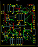
Thanks for all that wealth of great knowledge. I know this sound crazy and will put up a lot of questions of the type: "how could you sped that much time,?", "You know that it is almost useless?" and so on, but I have just spend over 10 hours in KiCad to make a sort of copy of prasi's design. And then asked FreeRouting to connect tre traces, as avtech23 did advice me🙂
FreeRouting do a strange job, but it tells me that everything connects, no via's.
avtech23 I do also like your design, simple and with a great seperation and wide traces.
I am trying to design so that the board can be connected to some side mounted heatsinks.
10 hours is slower then a snail, but 10 hours of fun and learning is, in my opinion, a great usage of time! 🙂
What I about to do now, is to manual rout the traces as avtech23 is recommending, and to make cirtain do I check on the calculator 00940 linked to.
Any comment before trying to trace the board?
I am aiming for getting something like prasi have done.
Thanks to you all!!! 🙂
Attachments
You are doing very well 🙂
You might want to look at making the resistors smaller. Only the 0.22 ohm and 10 ohm are large. I would also make the tracks thicker and pads larger.
Its good to print out a board layout and then it suddenly all looks more real and you will see how fine those traces really are 🙂
But you are doing great.
You are doing very well 🙂
You might want to look at making the resistors smaller. Only the 0.22 ohm and 10 ohm are large. I would also make the tracks thicker and pads larger.
Its good to print out a board layout and then it suddenly all looks more real and you will see how fine those traces really are 🙂
But you are doing great.
One thing I found invaluable in PCBCAD software is a "swap autoplacer."
It swaps same components around until it finds shortest net length.
Gives you the best chance of routing tight pcb's.
Pew great, that make me a happier. 🙂
I know that the resistors are big, I'll try to find smaller once🙂
How many wattage should I go for if into 45V as you write on the board, connected to 4 Ohm speakers?
What size of pads and tracks? Tracks are 3 mm now.
I know that the resistors are big, I'll try to find smaller once🙂
How many wattage should I go for if into 45V as you write on the board, connected to 4 Ohm speakers?
What size of pads and tracks? Tracks are 3 mm now.
What size of pads and tracks? Tracks are 3 mm now.
Tracks as big as possible, it costs nothing to leave copper on the pcb and improves trace impedance.
Pew great, that make me a happier. 🙂
I know that the resistors are big, I'll try to find smaller once🙂
How many wattage should I go for if into 45V as you write on the board, connected to 4 Ohm speakers?
What size of pads and tracks? Tracks are 3 mm now.
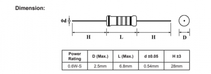
0.6 watt metal film are perfect. Most of the resistors dissipate under 5 millwatts and many dissipate only a few microwatts.
Only the 0.22 ohm and 10 ohm are bigger higher wattage parts.
Attachments

You are certain about that ? 3 mm is about 120mil, your tracks look to be about 24mil at first sight. 120mil is already pretty good in terms of width btw.What size of pads and tracks? Tracks are 3 mm now.
I would use the typical 0207 0.6W metal film resistors (6.3mm long, 2.4mm wide) for most places. In terms of layout, that translates best in pads spaced 10mm apart (or usually 0.4"), so that you don't bend the legs too close to the body of the resistor (you risk stressing them).
Btw, you'll quickly find out that most specs for pcb layout are expressed in mil (1/1000th of an inch) and the typical "grid" will be based on a 0.1" spacing. Old convention 😉
edit: beaten to it by Mooly 😉
Okay thanks, so in short largest feets and tracks, without using a square foot of pcb🙂
KiCad is shown measurements in mm and 3 mm is the standard track, with 0.5 spacing and 0.5 mm if its to the BJT's.
KiCad is shown measurements in mm and 3 mm is the standard track, with 0.5 spacing and 0.5 mm if its to the BJT's.
Sorry but a TO3P is 16mm wide. Your tracks are visibly way less than a 1/5th of the width of the mosfet.
Thank you a lot, I'll correct that... in some way🙂
By the way, I have tried 5 mm pads but that looks totally insane.
Am I missing something here: The pad has to be so big that solder is connecting perfect, but also not so big you have to use large amount of solder. That a 1 inch pad is not giving better connection then a i.e. 5 mm pad. That the only reason for bigger pads is to make space for larger tracks?
A visible improvement already FM.
You need to increase your track separation in the design rules. Look at the gap between the tracks at c11 for example. In reality that distance is going to be very small and cause issues .
Give the components some space - Q7 and R24 are overlapping. You need to ensure there is enough space to solder.
Try to use symmetry to your advantage - if your circuit has 2 channels, you can mirror most parts.
Aesthetically, try to line up components where possible or use the same offsets to make it easier to place tracks that traverse under a component. Plus a board that looks good often takes more thought and planning than one that is an autorouter jumble - it is more likely to be a better laid out board.
Thank you, I am about to lay last hand on changing all resistor sizes and shall then place traces, so you advice comes at a perfect moment🙂
I had some trouble sleeping yesterday so...
Not really tidied up and optimized but just another example, to show how to better make use of your two layers and maximize copper use.
The mosfet go "under" the pcb, in between the pcb and the heatsink, the leads bent upwards and the whole pcb is attached to the heatsink.
Dear 00940, Can you kindly post the project files for your layout of the mooly amp ? Both schematic and pcb ? I think it is in kicad !
--gannaji
While selecting components I search a lot in the original thread about Mooly's fantastic amplifier and some of the resistors have to non inductive = not wirewound, and that do make a lot of cense. But then do I stumble upon non inductive wirevound resistors??!! An inductor that is non inductive??
https://www.digikey.com/products/en?keywords=NKN3WSJR-73-0R22
Mooly's original post:
My MOSFET amplifier designed for music.
https://www.digikey.com/products/en?keywords=NKN3WSJR-73-0R22
Mooly's original post:
My MOSFET amplifier designed for music.
Hi Space,
All 0.6 watt metal film apart from all the 0.22 ohms which are 3 watt types, and these must be non inductive-- no wirewounds-- try and get the cermet or film types, and the 10 ohm in the Zobel network which is a 2 watt carbon type. Unless you plan on testing at high powers and at high frequencies 2 watt is fine. The only diode is the 12 volt zener and any 0.4 or 1.3 watt type is fine.
Build it exactly as per the circuit to begin with. If you need any advice or help just ask 🙂
When it's nearly done let me know and I will post how to test it so if there are any problems or errors it won't pop the outputs.
Use a preset for R8 at first.
- Home
- Design & Build
- Construction Tips
- Worst PCB track-layout ever?