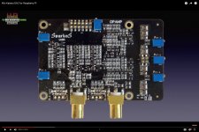
Katana Operational Amplifier Board
This is the operational amplifier board for the Katana (middle board on the stack). This board uses discrete circuits instead of integrated circuits. This is great for what they are doing, but we can't afford to do that (yet), so we'll stick to the OPA1612. What's interesting though is that the entire circuitry is on a separate board from the DAC board. Therefore, this answers a question that we had yesterday: we can put the op amps on a separate board without fearing too much degradation of the signal (as long as we believe that the Katana design works).
This is the operational amplifier board for the Katana (middle board on the stack). This board uses discrete circuits instead of integrated circuits. This is great for what they are doing, but we can't afford to do that (yet), so we'll stick to the OPA1612. What's interesting though is that the entire circuitry is on a separate board from the DAC board. Therefore, this answers a question that we had yesterday: we can put the op amps on a separate board without fearing too much degradation of the signal (as long as we believe that the Katana design works).
Attachments
e can put the op amps on a separate board without fearing too much degradation of the signal (as long as we believe that the Katana design works).
The Katana design works well with the ESS chip. However, this is another area where AK4499 may differ from Katana. First, I/V opamp outputs are routed through the inside of the dac chip which puts the dac chip inside the opamp feedback loop. We want that loop to be as physically compact as possible to avoid pickup of stray EM fields. The loop works at very high gain, and thus is very sensitive. Second, I/V opamp +-15v power sequencing is critical to avoid possible catastrophic damage to the dac chip, so great care is required in that respect.
Also, it occurs to me that so far there appears to be thought about protecting circuitry from insertion or removal of modules while the underlying system is powered on. That could also risk catastrophic damage to components.
Last edited:
Well, except perhaps that it first needs to be decided how the USB board will be clocked. Clocks are often located on it and used to help with re-clocking signals post-galvanic isolation. Or, clocks may be located externally from the USB board and the board configured to signal which of the two external clocks is needed to be enabled at any particular time.
This area is one where Katana differs from many dacs. Katana uses an ESS dac chip operating in master I2S mode, whereas AKM dacs don't support acting as I2S master.
Well, that was my original assumption. But then we have to make a decision: a chip can't be on two boards at the same time... Our USB interface will be provided by the STM32H743, which is mounted on what we call the plate PCB (bricks are mounted on the underlying plate, which is itself mounted on a tray). If we want, we could put the clock oscillator on the plate PCB, next to the STM32H743 MCU. But if we do that, the clock oscillator would be further away from the DAC chip, because we have the PSU board in between the MCU board (plate PCB) and the DAC board.
Therefore, my original idea was to put the clock oscillator on the PSU board. With that arrangement, there would be one set of connectors between the MCU and the clock oscillator, and one set of connectors between the clock oscillator and the DAC chip.
But I am totally open to any other arrangement that might make more sense.

The Katana design works well with the ESS chip. However, this is another area where AK4499 may differ from Katana. First, I/V opamp outputs are routed through the inside of the dac chip which puts the dac chip inside the opamp feedback loop. We want that loop to be as physically compact as possible to avoid pickup of stray EM fields. The loop works at very high gain, and thus is very sensitive. Second, I/V opamp +-15v power sequencing is critical to avoid possible catastrophic damage to the dac chip, so great care is required in that respect.
Also, it occurs to me that so far there appears to be thought about protecting circuitry from insertion or removal of modules while the underlying system is powered on. That could also risk catastrophic damage to components.
Great points!
If we want the op amps to be on the same board as the DAC chip, the only way that we can make them fit is to put them on the bottom side of the board, right underneath the DAC chip. But that means that we'll get a via to go from the DAC to the op amp, and another via to go from the op amp to the connector leading to the XLR board. Is that acceptable?
As far as removal of boards is concerned, this is impossible when the setup is powered on, because of the brick's frame and the way the four PCBs will be assembled together: The top cover will have threaded standoffs and the four PCBs will be secured by four socket head screws that go through boards 1, 2, and 3 and are fastened on the threaded standoffs of board 4 (the top cover board). In order to remove these screws, one will need to remove the brick from the plate, and doing so will shut the brick down.
Last edited:
...my original idea was to put the clock oscillator...
But I am totally open to any other arrangement that might make more sense.
Okay, let's think about it for a moment... Low clock jitter is essential for best dac performance. In that regard having both clocks close the dac chip seems a good idea (in fact, there could be four clocks used if 768kHz PCM compatibility is a requirement). In that case, clock signals could be distributed back to the USB board by something like: https://www.onsemi.com/pub/Collateral/NB3L553-D.PDF
...(don't forget bypass caps right at each device, and ideally, local voltage regulators for each clock module, and separate one for NB3L5533 device(s).
If needed to help restore signal quality, the local clocks could re-latch I2S signals from the USB board using something like: http://www.potatosemi.com/potatosemiweb/datasheet/PO74G374A.pdf
...don't forget local bypassing right at the device 🙂
Some decision would also need to be made as to which clocks will be used, since different brands may only come in certain physical sizes. NDK SDA are popular, but not the only possibly good choice for a high end dac.
Last edited:
Okay, let's think about it for a moment. Low clock jitter is essential for best dac performance. In that regard having both clocks close the dac chip seems a good idea (in fact, there could be four clocks if 768kHz PCM compatibility is needed). In that case, clock signals could be distributed back to the USB board by something like: https://www.onsemi.com/pub/Collateral/NB3L553-D.PDF
...(don't forget bypass caps right at each device, and ideally, local voltage regulators for each clock module, and separate one for NB3L5533 device(s).
If needed to help restore signal quality, the local clocks could re-latch I2S from the USB board using something like: http://www.potatosemi.com/potatosemiweb/datasheet/PO74G374A.pdf
...don't forget local bypassing right at the device 🙂
Ah, now we're talking!
Yes, having 768kHz PCM compatibility is highly desirable.
I'll work on schematics for all that as soon as I've made a clean inventory of all the parts that are needed.
Well, that was my original assumption. But then we have to make a decision: a chip can't be on two boards at the same time... Our USB interface will be provided by the STM32H743, which is mounted on what we call the plate PCB (bricks are mounted on the underlying plate, which is itself mounted on a tray). If we want, we could put the clock oscillator on the plate PCB, next to the STM32H743 MCU. But if we do that, the clock oscillator would be further away from the DAC chip, because we have the PSU board in between the MCU board (plate PCB) and the DAC board.
Therefore, my original idea was to put the clock oscillator on the PSU board. With that arrangement, there would be one set of connectors between the MCU and the clock oscillator, and one set of connectors between the clock oscillator and the DAC chip.
But I am totally open to any other arrangement that might make more sense.
I admit I have lost track of the overall architecture here, but I would suggest what I think Mark also said: clocks placed near converters, fed back to the USB receiver (STM32H7).
I happen to think the best approach is actually creating your own I2S bit clock and word clock (aka your DAC is the I2S master) divided from MCLK. Which is, I gather, what the ESS DAC does internally in the master mode that Mark mentioned. The advantage of this approach is you might, depending on the USB receiver, be able to avoid passing MCLK all the way back to the USB board and across an isolation barrier.
It won't really hurt performance if you have the STM32 be the I2S master, I am sure you can achieve the same result, it's just a lower EMI risk.
Last edited:
Some decision would also need to be made as to which clocks will be used, since different brands may only come in certain physical sizes. NDK SDA are popular, but not the only possibly good choice for a high end dac.
I am totally open to suggestions there. What I can tell is that the footprint of the NDK SDA should work based on our current constraints, and I'd like to go with an option that is known to work with the other components that we are going to use, because breadboard prototyping won't be an option for any of this.
I admit I have lost track of the overall architecture here, but I would suggest what I think Mark also said: clocks placed near converters, fed back to the USB receiver (STM32H7).
I happen to think the best approach is actually creating your own I2S bit clock and word clock (aka your DAC is the I2S master) divided from MCLK. Which is, I gather, what the ESS DAC does internally in the master mode that Mark mentioned. The advantage of this approach is you might, depending on the USB receiver, be able to avoid passing MCLK all the way back to the USB board and across an isolation barrier.
It won't really hurt performance if you have the STM32 be the I2S master, I am sure you can achieve the same result, it's just a lower EMI risk.
That makes sense to me. So, without going into too many details right now, the conclusion seems to be that the 2 or 4 clocks are sitting really close to the DAC chip, on the same side of the board (board #2). And these clocks will be shielded for good measure.
So far, so good...
Yes! It's 0.5mm tall instead of 0.9mm, but that should not make any difference for our modeling, at the exception of shielding perhaps, but we'll make sure to take that into account in due time.
Thanks!
Thanks!
Both books are in the mail!
Just received my copy of Electromagnetic Compatibility Engineering by Henry W. Ott. This stuff is solid gold! And the writing is super clear. Many thanks to Mark for his numerous recommendations. Once I'm done with it, I'll read The Art of Electronics, then read Ott again.
Cheers!
Making the DAC brick larger
Okay, I gave it a shot, but I failed, and it's not for lack of friendly warning... To make a long story short, there is no way to fit all the components that we need for the DAC brick within a 35mm × 35mm footprint. It simply won't work, mostly because of the electrolytic capacitors. Even with tantalum capacitors, I doubt that it could be done, and I would like to stick with electrolytic capacitors, because their discharge characteristics are known to work for AKM's reference design, and I do not want to take any chances. Furthermore, I am concerned about heat dissipation with 4 PCBs stacked within 30mm of height...
Unlike other DAC designers, I am not trying to improve upon the AKM reference design. Instead, I am just trying to make this design fit within a smaller form factor, while using a different USB interface. Therefore, the closer we stick to the reference design, the higher a chance we have to make it work and sound good. It might not sound the best in its first version (it won't), but I'll be happy if it sounds just good, because there is probably very few commercially-available products that could sound much better within such a tight package.
So, with that in mind, we've decided to move to a two-unit brick, meaning 76mm × 38mm for the brick, or 73mm × 35mm for the PCB. And if that still does not work, we will move to a three-unit design. But with a two-unit design, we would be able to fit three of these bricks on a plate, plus three single-unit bricks with bargraphs (I really want a bargaph close to every audio input or output). And it will allow us to output each of the four mono channels through a dedicated Mini XLR port. Here is what a reference setup would look like with twelve plates, each populated with three DAC bricks and three bargraph bricks (rows 1 and 2 on the spreadsheet).
Now, this change has its benefits. Among them, the fact that we can now dedicate a full STM32H743 MCU to each and every DAC brick (the bargraphs won't take much), without having to worry about whether we have enough power to handle all the audio channels that would need to be processed if we were to use three DAC bricks per MCU. Another benefit is that bargraphs for these audio outputs will now be packaged within a separate brick, which should help reduce interferences with the components housed by the DAC brick.
With these dimensions, we can probably have a layout for the DAC board that is very close to the layout used on the AKM reference design's mezzanine board (the one hosting the DAC, with its schematic on page 58): the OPA1612's could be on the same side of the PCB as the DAC chip, and the 8 large capacitors could be mounted very close to the DAC chip, with 4 on each side of the board. The only deviation from this design would be the mounting of the 19 smaller 10µF capacitors, which would probably have to be mounted on both sides of the board, thereby requiring some traces to go through single vias, but I don't see how this could be a show stopper.
Sorry for my stubbornness: I had to give it a try.
Last edited:
Exposed Pad for AK4499EQ
I am trying to figure out the geometry for the PCB pad corresponding to the exposed pad of the AK4499EQ. As can be seen on page 114 of its datasheet (downloadable upon registration), its dimensions are 8.1mm × 6.6mm. I found a recommended land pattern on this Intersil document, but it does not specify the dimensions of the middle pad, which appear to be chip-specific. And this NXP Mechanical Outline for the SOT1522-1 isn't much help either. What is a best practice for this kind of pad?
I am trying to figure out the geometry for the PCB pad corresponding to the exposed pad of the AK4499EQ. As can be seen on page 114 of its datasheet (downloadable upon registration), its dimensions are 8.1mm × 6.6mm. I found a recommended land pattern on this Intersil document, but it does not specify the dimensions of the middle pad, which appear to be chip-specific. And this NXP Mechanical Outline for the SOT1522-1 isn't much help either. What is a best practice for this kind of pad?
Pad on board should be a tiny bit larger than the pad on chip to allow for solder alignment, same as whatever the pins have relative to their solder pads is probably good. Also, presume you saw orientation of the pad relative to pin-1.
Last edited:
Pad on board should be a tiny bit larger than the pad on chip to allow for solder alignment, same as whatever the pins have relative to their solder pads is probably good. Also, presume you saw orientation of the pad relative to pin-1.
Thanks! Yes, I saw it. I got confused at first, but after a 90 degrees rotation, everything was fine.
DB2132000L Replacement
The DB2132000L used for D1..4 is marked as "End of Life" by Mouser. Any recommendation for a suitable alternative?
And how on Earth can a brand-new evaluation board use EoL components? This is beyond me...
The DB2132000L used for D1..4 is marked as "End of Life" by Mouser. Any recommendation for a suitable alternative?
And how on Earth can a brand-new evaluation board use EoL components? This is beyond me...
Last edited:
- Home
- Source & Line
- Digital Line Level
- 8 × AK5578EN + 8 × AK4499EQ ADC/DAC Boards