Since Groner's circuit is, in any practical audio sense, totally without noise or distortion, are there any initial audition impressions anyone wishes to report?
Yep. I gave a link to a complete PDF in #72.
My proposal in #67 differs in that the tracking source is the input signal, not the output signal. If we only want to track the rails output as source is OK, but to avoid output voltage swing of the control amp (which may cause additional distortion) we must use the input signal to force the slave amp (-)Input voltage which defines master amp output voltage. We can't use a divider from the output for this as this would take down the slave gain, now running in low fixed gain hookup.
As mentioned, the idea is to lock down the master opamp's input and output voltages to zero (AC) in any circuit config so that the only fluctation seen is the tiny voltage to drive the (quasi open-loop) slave amp. The master amp always works under inverting operating conditions. An inverting mode emulator of sorts.
Apologies on missing your subsequent link, but probably better to have it twice rather than not at all.
Cool idea; perhaps I'm confused (very likely), but doesn't this essentially force the control opamp to run in unity gain? I understand the overall goal to track input to achieve essentially zero common mode on the control opamp, minimizing those distortion mechanisms.
Similarly, isn't one of the major advantages of a composite, at least at low frequencies (audio), that the combined loop gain mean that all the large signal amplification happens in the output amplifier (in that quasi open loop that you describe). This obviously requires careful shaping of the local feedback loops to jam as much of the loop gain into the outer loop. Differential voltage on the inputs gets minimized, but I suppose that does leave the common mode voltage intact.
I'll keep scratching my head about the idea, nonetheless.
Just to be clear, you did add a 10 Ohm resistor from the 1st amplifier output to grond? Because that is what prevents to output lockup in the first place (at power on) and consequently the slow recovery. Any way I was just wondering ...
No, no 10R, just the schematic as posted in the 1st post, but without the diodes & without the 1k. That is unstable.
Jan

No, no 10R, just the schematic as posted in the 1st post, but without the diodes & without the 1k. That is unstable.
Jan
O.k. that is what I understood initially.
Then I did read the paper.
And then I wondered if the diodes network could be replace by one resistor 🙂
Last edited:
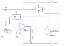
Because we are at composites, here's an idea I had a few years ago, while looking for an ideal opamp for a high purity oscillator based on Jim Williams design. Worked great for that, in a prototype.
It's an inverting configuration (ideal for low distortions), shown for a LF gain of -1.
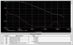
Attached is also the simulated loop gain and phase, almost 200dB LF loop gain, 50 degrees phase margin and an ULGF of 130MHz. 113dB of loop gain @60KHz, which explains why I was not able to measure any oscillator distortions @20KHz and 5V output in a 600ohm (didn't bother to try below -140dB).
I'll try to revive this little project and do some loop gain measurement (now I have the means, didn't have at that time).
It's an inverting configuration (ideal for low distortions), shown for a LF gain of -1.
Attached is also the simulated loop gain and phase, almost 200dB LF loop gain, 50 degrees phase margin and an ULGF of 130MHz. 113dB of loop gain @60KHz, which explains why I was not able to measure any oscillator distortions @20KHz and 5V output in a 600ohm (didn't bother to try below -140dB).
I'll try to revive this little project and do some loop gain measurement (now I have the means, didn't have at that time).
Attachments
OK, so ideally R1, C1 and R4 already define the gain you want to have. Due to finite gain of U7, there is some error that the outer loop via U6 corrects for. R2, C2 and R3 set the closed-loop gain of this outer loop. I guess the loopgain you simulated applies to U7, not to U6.
How sensitive are you to a bit of mismatch between the inner and outer feedback networks?
How sensitive are you to a bit of mismatch between the inner and outer feedback networks?
Last edited:
If you image the bootstrapped version set up in inverting config you'll see that nothing changes for the gain structure compared to the standard version. There just is a buffered GND now (pretty much useless), for the secondary GND connections of the compensation network. Therefore, transfering the circuit into non-inverting works equally well as it does with a single stage, it's only naming convention of what we call input, output and reference nodes, after all.Cool idea; perhaps I'm confused (very likely), but doesn't this essentially force the control opamp to run in unity gain? I understand the overall goal to track input to achieve essentially zero common mode on the control opamp, minimizing those distortion mechanisms.
Similarly, isn't one of the major advantages of a composite, at least at low frequencies (audio), that the combined loop gain mean that all the large signal amplification happens in the output amplifier (in that quasi open loop that you describe). This obviously requires careful shaping of the local feedback loops to jam as much of the loop gain into the outer loop. Differential voltage on the inputs gets minimized, but I suppose that does leave the common mode voltage intact.
I'll keep scratching my head about the idea, nonetheless.
----------
Any composite is limited by it first input stage parasitic errors no matter how high we drive the open loop gain and how linear the feedback components and how perfect the layout. PSRR, CMRR, themals, internal crosstalk, etc quickly dominate the error budget, then. That's why it is essential to give the control amp the best operation conditions.
Risking a shot from the hip, I would think a few % won't matter much. Actually we could inject a little external error current at the slave summing node with no change in performance. Basically the (-)in's are sort of tied together, similar to the Soliman composite (don't find a reference right now). But maybe I'm wrong...How sensitive are you to a bit of mismatch between the inner and outer feedback networks?
... quick sim with a similar config shows no severe problem when the compensation is correct to begin with, even with 10% component variation for the slave feedback's R's and C. DC gain suffers the most and GBW moves around by a factor of 1.5 or so.
By the way, I think the Groner circuit would also be great for a low distortion two-integrator oscillator. For example, start with a circuit like in the first post of this thread: Any opinions or improvements suggestions for this low THD 1kHz sine generator?
Replace the op-amps in the loop (integrators and inverting amplifier) with Groner-style composite op-amps. The compensation may have to be redimensioned for the inverting amplifier because of the attenuation of its feedback network. Use very good capacitors for the integrators.
As the op-amps will cause practically no phase shift at the oscillation frequency due to their huge loopgains, the amplitude control branches can hopefully be made a lot weaker (provided you don't mind when start up takes some time). R3 and R5 can then be increased a lot and possibly the JFET can be replaced with a LED optocoupler, similar to the Jim Williams Wienbridge circuit ( https://www.edn.com/design/analog/4368298/Test-18-bit-ADCs-with-an-ultrapure-sine-wave-oscillator ). You could even consider cutting out R5-R4-J1 altogether and replacing R3 with a T-network with an LDR in the middle.
Risking a shot from the hip, I would think a few % won't matter much. Actually we could inject a little external error current at the slave summing node with no change in performance. Basically the (-)in's are sort of tied together, similar to the Soliman composite (don't find a reference right now). But maybe I'm wrong...
Correct, up to 5%-10% mismatch is no problem, just enough to be able to adjust the gain using a LDR per Jim Williams schematic. The change in the stability margin is minimal.
BTW, if not clear, this is a pole-zero cancellation schema (or I prefer to look at it this way). I have somewhere the full analytic (pen on paper) derivation of this pole-zero cancellation technique, algebra is not for the faint of heart though. I'll dig for it if there's somebody interested. The cancellation condition is K=R1/R2=C2/C1=R4/R3. Any K between 4 and 10 will do just fine.
This composite is stable for any (inverting) closed loop gain.
P.S. I replied before reading your other message. Yes, a mismatch impacts mostly the ULGF and not the stability.
I guess the loopgain you simulated applies to U7, not to U6.
How sensitive are you to a bit of mismatch between the inner and outer feedback networks?
For loop gain, the global loop is broken at the U7 output. There's a (multiloop feedback) theorem that says you can do that for global stability analysis, no need to check both loops separately. If memory serves, this theorem is discussed in the Middlebrook GFT context.
Sensitivity discussed above.
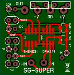
SG Super Opamp in pro audio 2520 pinout
I have been playing about crafting a PCB layout for this opamp. It lends itself well to the old timey 2520 socket footprint found in pro gear. Circuit ground is part of the standard. I think that I will fab a few PCBs and see how well they work.
I have been playing about crafting a PCB layout for this opamp. It lends itself well to the old timey 2520 socket footprint found in pro gear. Circuit ground is part of the standard. I think that I will fab a few PCBs and see how well they work.
Attachments
Last edited:
Correct, up to 5%-10% mismatch is no problem, just enough to be able to adjust the gain using a LDR per Jim Williams schematic. The change in the stability margin is minimal.
I was wondering more about the distortion than about stability. The first op-amp has to produce a larger correction signal with feedback network mismatch, how does that affect the distortion of the whole thing?
BTW, if not clear, this is a pole-zero cancellation schema (or I prefer to look at it this way). I have somewhere the full analytic (pen on paper) derivation of this pole-zero cancellation technique, algebra is not for the faint of heart though. I'll dig for it if there's somebody interested. The cancellation condition is K=R1/R2=C2/C1=R4/R3. Any K between 4 and 10 will do just fine.
I'm definitely interested (and I'm used to transfer function calculations with lots of terms).
For loop gain, the global loop is broken at the U7 output. There's a (multiloop feedback) theorem that says you can do that for global stability analysis, no need to check both loops separately. If memory serves, this theorem is discussed in the Middlebrook GFT context.
The loop gain seen from the first op-amp is much smaller, so its distortion is suppressed less - but then again it has an almost zero output signal, so it probably doesn't distort much to begin with.
O.k. that is what I understood initially.
Then I did read the paper.
And then I wondered if the diodes network could be replace by one resistor 🙂
I think if you would look at the schematic of the 211 in the data sheet, it is apparent that a load resistor of 10 ohms would kill most of the OL gain.
Jan
I have been playing about crafting a PCB layout for this opamp. It lends itself well to the old timey 2520 socket footprint found in pro gear. Circuit ground is part of the standard. I think that I will fab a few PCBs and see how well they work.
Carl, you don't like SMT? Those components can be got in SMT shape with very good quality, film R's, film caps. I used size 0805 throughout, which is not hard to solder after a couple of throw-away tries.
BTW, Samuel recommends a resistor between the power supplies to the opamps, so that the signal-induced power supply ripple on the output opamp would get attenuated on its way to the power supply of the input opamp. So connect the power first to the output opamp with decoupling, then via a resistor to the input opamp and also local decouple it. Everything matters at -180dB.
I didn't do that in my implementation but you may want to put the provision on your PCB.
Jan
Last edited:
That takes a little bit of space too on an adaptor.So connect the power first to the output opamp with decoupling, then via a resistor to the input opamp and also LOCAL DECOUPLE it.
Jan
OK, K is just impedance scaling, for convenience bascially.BTW, if not clear, this is a pole-zero cancellation schema (or I prefer to look at it this way). I have somewhere the full analytic (pen on paper) derivation of this pole-zero cancellation technique, algebra is not for the faint of heart though. I'll dig for it if there's somebody interested. The cancellation condition is K=R1/R2=C2/C1=R4/R3. Any K between 4 and 10 will do just fine.
This composite is stable for any (inverting) closed loop gain.
What is the advantage over the simpler Soliman topology where only one copy of the feedback network is used, feeding both (-)in's?
Carl, you don't like SMT? ... Jan
I work with surface mount when I absolutely have too. I don't enjoy it as much as I do thru hole. I suppose I am conceding to old habits. But in this case I felt obligated to use thru hole. Somehow using SMT on such an 'old school' footprint just seemed well, sacrilegious. Ha, ha ...
And thanks for the advice on improving the power feed to the opamps!
Go vertical and don't try to be DIP8 pinout compatible (makes no sense as you need the explicit GND, preferably two actually, plus this is not a candidate for opamp rolling). Or/and use small footprint OpAmps, no need to waste space with huge SO-8 etc. OPA211 in VSSOP-8 and THS4031 in MSOP-8. You could also stack boards. There are ways....That takes a little bit of space too on an adaptor.
- Home
- Source & Line
- Analog Line Level
- Samuel Groner's super opamp