Almost did an Econowave a few years ago.
May have to get back into speakers some of these days.
What have you been driving the Enzo's with?
May have to get back into speakers some of these days.
What have you been driving the Enzo's with?
I don't think you have a blown fet, but a bad solder joint, misplaced component or bad connection.
I don't think you have a blown fet, but a bad solder joint, misplaced component or bad connection.
I will closely check the above when I get the board back out before pulling any fets.
Almost did an Econowave a few years ago.
May have to get back into speakers some of these days.
What have you been driving the Enzo's with?
I have had F5, but usually BA3. AlephJ and M2 work very
well also. AlephJ J very nice!
Russellc
Everything but the kitchen sink and your F6.
Glad to hear of a Tekton working well with a variety of Firstwatt amps as I have
plans for an M2x and likely a SissySIT after the AJ.
Glad to hear of a Tekton working well with a variety of Firstwatt amps as I have
plans for an M2x and likely a SissySIT after the AJ.
I used the AJ transistor kit from the diyAudio store which shows part numbers
ZTX450 and ZTX550, and those are the numbers on the parts supplied.
ZTX450 and ZTX550, and those are the numbers on the parts supplied.
Everything but the kitchen sink and your F6.
Glad to hear of a Tekton working well with a variety of Firstwatt amps as I have
plans for an M2x and likely a SissySIT after the AJ.
I cannabilized the F6 to build AlephJ. Never looked back.
Russellc
I used the AJ transistor kit from the diyAudio store which shows part numbers
ZTX450 and ZTX550, and those are the numbers on the parts supplied.
I know on Pearl II projects people have had problems in the past with the ZTX450 going bad due static electricity before/during installation. Maybe you should try replacing all three ZTX components.
I know on Pearl II projects people have had problems in the past with the ZTX450 going bad due static electricity before/during installation. Maybe you should try replacing all three ZTX components.
Has there been found enough difference in the ZTK's from different mfgr.s to make it desirable to match by the maker?
Mouser and digikey have them made by Diodes Inc, Zetex can be had on ebay.
I sent an info request to Jason to see if he had some more he could sell and could ID the mfgr of the ZTK's supplied in the kits.
Guess I could replace them in both boards if need be. Hate to mess with the one that is working, though.
.....
Guess I could replace them in both boards if need be. Hate to mess with the one that is working, though.
considering role of bjts in Aleph amp , you can put different types in two channels , and there will not be any sound difference ..... maybe even not measured one
so , leave functional channel as is and work on bad one
remove JFets , check them with simple JFet matching jig ( 9V battery and mAmeter)
triple check values of all resistors , compare placement to both schematic and functional channel
recheck source resistors of mosfets
check isolation (electrical) between mosfets and heatsink
check tightness of mosfet screws
check bjts (pinout , orientation , type) , replace them if there is anything suspicious
check all wires , check everything for shorts , check all solder joints visually , reflow if suspicious
check trimpots ( if you have any) with ohmmeter .... compare measurement with good channel
all of above , as general guides .....
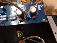
I managed to pull the trace "eye" from the V+ wire entry during the course of my in/out, reflow, double checking efforts.
This was after the symptoms board #1 has been exhibiting were 1rst observed.
I don't see a continuing trace on the front, but thought I should make this known in case I'm mistaken and have compounded the troubles.
This was after the symptoms board #1 has been exhibiting were 1rst observed.
I don't see a continuing trace on the front, but thought I should make this known in case I'm mistaken and have compounded the troubles.
Attachments
no big deal , if you lifted upper pad copper
what counts is that wire is having proper contact with trace beneath
what counts is that wire is having proper contact with trace beneath
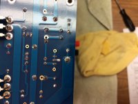
In the second photo showing the bottom, in some places it looks like you need to be using flux, and some of your solder joints are nearly (or are) missing the pad completely.
I picked up a $15 strap-on-your-head magnifying lens, and was shocked at how much worse my solder joints looked under magnification.
I picked up a $15 strap-on-your-head magnifying lens, and was shocked at how much worse my solder joints looked under magnification.
Attachments
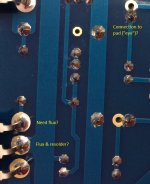
After looking at the picture I submitted and noticing the same thing you did, I filled the pads with solder on the back, the fronts were all full.
Also drew the solder up the mosfet legs as best I could.
Using good old Kester 44, I just didn't put all the solder on those mosfet pads that could be put.
I'm going to follow your advice and get some magnification to use for inspecting solder joints. At work there used to be some dandy 4" diameter ones mounted on a flex arm that I think is what I need, so off to Google in search of same.
Not really, aside from reasonably well-matched and BL grade (6-12mA Idss) ‘
The CCS in the circuit controls the Jfets more than their Idss
Hi,
Does it follow then that I can go ahead and use V grade Toshibas matched at 11 mA Idss?
Thanks
yup
just as addendum .....
for 2SJ74 (and 2SK170):
GR grade being declared as current range of 2.6mA-6.5mA
BL grade being declared as current range of 6.0mA-12.0mAmA
V grade being declared as current range of 10.0mA-20.0mA
just as addendum .....
for 2SJ74 (and 2SK170):
GR grade being declared as current range of 2.6mA-6.5mA
BL grade being declared as current range of 6.0mA-12.0mAmA
V grade being declared as current range of 10.0mA-20.0mA
Last edited:
- Home
- Amplifiers
- Pass Labs
- Aleph J illustrated build guide