Sunny22G you can back read post 770 and 810.
Greetings sir U mean 100pf. I add on PCB..same problem
Greetings sir U mean 100pf. I add on PCB..same problem
Hi Sunny22g,
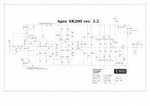
See the placement of 18pf compensation cap. Hope this helps.
Attachments
Hi Sunny22g,
See the placement of 18pf compensation cap. Hope this helps.
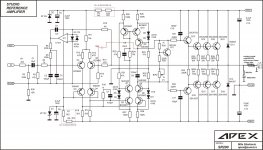
Schematic Sunny used for his build is shown in post #2794 - 18pF is already there.
Schematic Sunny used for his build is shown in post #2794 - 18pF is already there.
1.Then try change C23 with 1,5nF and R49 with 180-220R
2. Add 15-22pF from Base Q6 to collector Q8
3.Increase C8 or C22 to 10uF/16V+
4.Increase C10 and C11 to 150pF
BUT First-of-All
recalculate or measure voltage drop on R27 and R28 so we`ll find VAS bias on those 100R resistors!
LTP bias =(15V/5K/2)=3mA/2 = 1,5mA per BJT in input diff.pair = OK
R16, R17 voltage drop = 1,5mA*3K3 =4,95--->5V
VAS bias = (5V-Vbe_Q5)/100R = 4,3/100=43mA??? not OK!!!
dissipation of caskode Q8 and Q7
will be then aprocs. 50V*43mA=more then 2W , this ends as very-very hot VAS bias
Decrease value for both R16 and R15 from 3K3 to 910R-1,2K
so we get then R27, R28 bias close to 12-10mA
with dissipation of Q8 and Q7 and Q9 now: P_diss=50*10mA=>0,5-0,6W
diodes strings D5+D5, D8+D9, D10+D11 will work with 1-1,2mA bias
so we ends with VAS bias <10mA
Now first turn trimmpot R18 to max value so we get at start minimum BIAS,
Short input to SignalGND
Put Dummy load 4-10R (several W) on output
Power up the amp with limiter resistors (15-20R, several W) on rails,
then readjust R18 to read on DMM voltage drop on R39 (or on another output BJT emmiter resistors) those racomanded 22-25mV
= 23,5mV/0,33R = 70-75mA BIAS per output BJT pair
readjust bias after 10-15min amp idle runing.
Measure DC offset at output : +/-10mV OK
Control temperature of Main Heatsink, VAS Caskode BJTs Q7, Q8, Q9
Last edited:
Guys do u think . can I made this amplifier again or not ? I hope u understand my feelings. Sry for imba bad english
Guys do u think . can I made this amplifier again or not ? I hope u understand my feelings. Sry for imba bad english
Sunny22g,
it's your willingness to learn would decide. there are a lot of people who are willing to help you grow, you just have to understand and perform their advises- repeat it several times if necessary so you can learn.
Like you i have ask so many questions before but some of those questions had been answered in the past already so may i suggest to read the forum from the start as i did.
about 3 years ago i have started electronics from just googling ideas about amps my first amp was from Columbian websites - it works great, then made leach amps still it work. and now that i have found APEX by Mr. Mile its not just great when we talk about QUALITY and POWER.
i have made a lot of his designs with all has astonishing results. I have started with B500 next was AX14, FH9, SR200 with reversed version, SR250, AX14 3&4pairs, H900, pre-amps. active and passive crossovers and even speaker boxes.
and these people who helped you are the same people who helped me namely Sir Mile, Sir Dragan100, *AndrewT*, vzaichenko and a lot more...
to the D.I.Y. community THANK YOU for the help and support to the beginners i may not become expert nor earn profit but i have fulfilled my Hobby...
God Bless us all... ... ...

1.Then try change C23 with 1,5nF and R49 with 180-220R
2. Add 15-22pF from Base Q6 to collector Q8
3.Increase C8 or C22 to 10uF/16V+
4.Increase C10 and C11 to 150pF
BUT First-of-All
recalculate or measure voltage drop on R27 and R28 so we`ll find VAS bias on those 100R resistors!
LTP bias =(15V/5K/2)=3mA/2 = 1,5mA per BJT in input diff.pair = OK
R16, R17 voltage drop = 1,5mA*3K3 =4,95--->5V
VAS bias = (5V-Vbe_Q5)/100R = 4,3/100=43mA??? not OK!!!
dissipation of caskode Q8 and Q7
will be then aprocs. 50V*43mA=more then 2W , this ends as very-very hot VAS bias
Decrease value for both R16 and R15 from 3K3 to 910R-1,2K
so we get then R27, R28 bias close to 12-10mA
with dissipation of Q8 and Q7 and Q9 now: P_diss=50*10mA=>0,5-0,6W
diodes strings D5+D5, D8+D9, D10+D11 will work with 1-1,2mA bias
so we ends with VAS bias <10mA
Now first turn trimmpot R18 to max value so we get at start minimum BIAS,
Short input to SignalGND
Put Dummy load 4-10R (several W) on output
Power up the amp with limiter resistors (15-20R, several W) on rails,
then readjust R18 to read on DMM voltage drop on R39 (or on another output BJT emmiter resistors) those racomanded 22-25mV
= 23,5mV/0,33R = 70-75mA BIAS per output BJT pair
readjust bias after 10-15min amp idle runing.
Measure DC offset at output : +/-10mV OK
Control temperature of Main Heatsink, VAS Caskode BJTs Q7, Q8, Q9
Hello Sir , please tell me where I got R49. I cannot see this. Plz tell me thanks Sry for bad english
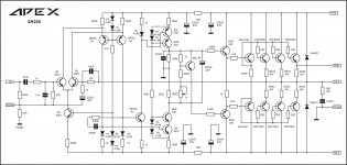
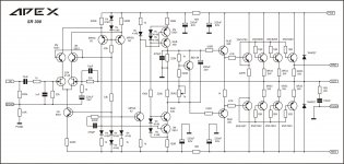
R49 is a part of the IPS compensation network to the right and a little bit down from Q4.
Sunny, why can we find it but you can't? 😉
Sunny, why can we find it but you can't? 😉
Hi Sunny22g,
See the placement of 18pf compensation cap. Hope this helps.
Lead and lag comp. on this topology ??
Dragon was right , but 33-47pf from
C Q8 to B Q6 - just simple miller comp.
Faster Q8 and 9 , not high cob slow mje340-350 - maybe even C4793/A1837.
Get rid of the 18pf/ and R18-C7
"abomination".
OP stage - huge 220R base-stoppers on the drivers ? Gone , add 5-10R base-stoppers to all the output devices.
With above alterations , <1mhz unity gain with @ 80 degrees phase margin can be
expected. (super stable with even enough derating to allow "junk drawer" semi's ).
Not to denigrate the design , but it ignores many of the audio design rules
laid out in both the Self and Cordell books ???
OS
Last edited:
I dropped my dream to make apex sr200. But droping sr200 . because there are many problems.... aur there are no diy member in my city.who can help my problems . I really love this amplifier because my friend have studio monitor . sound quality is very imba but I cannot full fill my dream s.
Last edited:

Hello I am totally confused.
Remove C7 (470pF), connect 47pf from C Q8 to B Q6, do not use 18pF (I can not see it on your build)...
Hello Sir , please tell me where I got R49. I cannot see this. Plz tell me thanks Sry for bad english
I sunny, you should see this diagram. And be cool 🙂)
Attachments
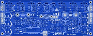
Sr200
Sir kandimba I will uploading 3.2 Ver .sir Juan give this zip there is PCB pictures.plz tell me where r49.
I sunny, you should see this diagram. And be cool 🙂)
Sir kandimba I will uploading 3.2 Ver .sir Juan give this zip there is PCB pictures.plz tell me where r49.
Attachments
- Home
- Amplifiers
- Solid State
- Studio Reference Amplifier