Hello All. Sorry to interrupt proceedings but I have a quick question for Mark. What differential amplifier did you use at the balanced output of the D/A chip?
All the opamps I am currently using for the project are OPA1612. Since they are SMD parts, I have them soldered to Brown Dog DIP adapters. Actually, you can order them with pins installed and an OPA1612 already installed: SO8 to DIP8 Adapter | BrownDog 970601 | Cimarron Technology
A total of four of the opamps are needed. Three for the output stage and one for the AVCC board. If one wanted to make a balanced output for each channel or otherwise add some more buffered gain, you would need two more for a total of six.
EDIT: Also, just to clarify, we don't directly use a differential amp for the outputs exactly. We use opamps as transimpedance amplifiers (current to voltage converters, or I/V) as the first part of the output stage for each of the dac outputs. The next opamp after that is a differential summing amplifier/reconstruction+HF_noise filter. That is where the balanced output signals get unbalanced. After that if one wanted to rebalance the filtered outputs, an opamp single-ended to balanced converter could be used.
Last edited:
Mark - Speaking of AVCC... What Twister Pear regulator they offer would work best for the 38q2m? IOW, which one do I need?All the opamps I am currently using for the project are OPA1612. Since they are SMD parts, I have them soldered to Brown Dog DIP adapters. Actually, you can order them with pins installed and an OPA1612 already installed: SO8 to DIP8 Adapter | BrownDog 970601 | Cimarron Technology
A total of four of the opamps are needed. Three for the output stage and one for the AVCC board. If one wanted to make a balanced output for each channel or otherwise add some more buffered gain, you would need two more for a total of six.
EDIT: Also, just to clarify, we don't directly use a differential amp for the outputs exactly. We use opamps as transimpedance amplifiers (current to voltage converters, or I/V) as the first part of the output stage for each of the dac outputs. The next opamp after that is a differential summing amplifier/reconstruction+HF_noise filter. That is where the balanced output signals get unbalanced. After that if one wanted to rebalance the filtered outputs, an opamp single-ended to balanced converter could be used.
redjr,
It is the one called, "AVCC-SR Dual 3.6V Series Regulator Module," on the following web page:
Trident-SR
Also, looks like they might have a few left of their old version called, "AVCC Dual 3.6V Shunt Regulator Module," on this page: Trident
I don't know the exact differences between the two or how they might differ in sound quality. I believe another Sabre dac manufacturer called Acko makes an AVCC regulator pretty similar to TP's AVCC-SR version. Acko says they compared their's to the ESS ES9311Q AVCC part, and they say the two don't sound much different. I guess the safe thing to do would be to go for the newer, more expensive AVCC-SR.
It sure would be nice though if someone who has the opamp version we are now using could also get a TP AVCC-SR and see if they sound any different. I guess I will have to do it myself eventually, but no time right now.
Last edited:
Hi Markw4,
Tried learning to design custom PCB with easyeda for, 1763-ldo, AVCC and Output Stage mode as per your mode(Bih schematic). Got to thinking if we have the schematic for the remaining parts on the chinese board(mine is the blue one) and re-design the complete board, it might take the same effort and time. The benefits I guess would be many. Although I understand that de-soldering and re-soldering of the DAC and microcontroller would be difficult and fair chance of destroying them. Just curious if there is a schematic for the board somewhere.
By the way, I got the Mouser parts, waiting for the prototype board from Aliexpress, no telling when I'll get them.
I did the 4.7uf DVCC cap mod and the clock. I could hear a definite improvement on the clock mod.
Regards,
Kay.
Hi Kay,
To my knowledge there is no complete schematic for any of the dac boards we use. In addition, there are some small differences between different versions of the boards. It is also possible that we will need to use one of the dac chip GPIO pins differently than the Chinese boards currently do. That could be designed around so that no loss of existing functionality would occur.
Regarding dac chip and MCU, if we made complete boards we would probably just buy the dac chips from an ESS distributor. They cost about $15 each in small quantities. The main thing about them is that they have a hidden solder pad on the bottom that needs to soldered in an oven, something a board manufacturer might be able to do for us just for that chip. We could also write our own MCU code which isn't very hard to do, so we could use almost any 3.3v MCU we might want.
The boards we see today are version 1.07 which means they have gone through seven design iterations as new features are added and other improvements made. I don't know exactly how a final board design might look yet. We are likely pretty close to knowing, but it could be we would still need to use multiple boards in some way.
Getting the AK4137 chip on the same board as the dac might be a very good goal. It is another chip that probably has to be cooked to solder a pad on the bottom.
For various reasons you can probably see from the above, I don't think we are probably quite ready for a final board design. A more practical shorter term goal might be to reduce some of the hand construction work that might deter people from starting on a dac modding project. An output stage board and maybe an AVCC board might make a lot of sense. Before embarking on an AVCC board, I would probably want to test ADM7150 type AVCC solutions like the TP one, to see if it would do just as well as what we use now. I think the current AVCC design is fine, except for the huge film caps. An SMD film cap for LT6655 would probably make a lot more sense. Also, probably make sense to compare film caps vs electrolytics to see if they make any difference at the the opamp outputs. Based on all that, I don't think we are ready even for an AVCC board without doing some more investigation. Since no one else but me has come far enough with actually building a modded dac, there is no one but me to do any experiments to find out what would make for a good AVCC board design.
The only part that we can say for sure is okay would probably be the output stage, and even that might get a small mod at some point in the future to tweak noise, filtering, gain, etc. However, having just an output stage PCB would be a big step forward for those interested in modding. Probably better for it to be SMD though, or stand-up through hole rather than lay-down-flat through hole.
Then people could buy a dac board from China, maybe an AVCC board from TP (if we find we like it), an output stage board of the group's design, and an AK4137 board. There would be a power supply of some type too, of course.
Regarding the AK4137 board, there may end up being some mods on that, don't know yet.
Its probably becoming more and more clear this whole dac thing is a work in progress, not a final design. The more active members of the group building and working on dacs probably the better. Right now its a lot to take on, and just finishing one would probably be enough for most people for awhile. It might be only a few that eventually get an itch to try to help with further development and refinement after fully modding one and getting it up and working.
Regards,
Mark
Last edited:
Mark,
Thanks for the detailed refresher. Can't wait to try the mods. Happy modding, you got a lot to do. Cheers.
Thanks for the detailed refresher. Can't wait to try the mods. Happy modding, you got a lot to do. Cheers.
Just found out dac chip GPIO output is going to need a buffer to drive the clock divider experiment. I have some parts on hand just in case that turned out to be necessary. Time to fabricate another little board, looks like. Oh, well. Other things seem to be working okay, such as the AK4137 board and dac board after their recent minor mods. Also, looks like the PC interface to control clock divider chip is working okay. Probably, it will be another couple of days before the next go at it.
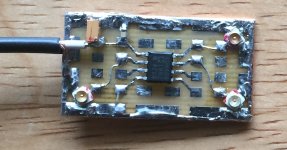
Just finished constructing a little LVCMOS to LVDS transmitter for driving the clock divider chip. It uses an ADN4661 High Speed Differential Driver. Also, considered using what looks like a possibly better choice, MAX9112 LVDS Line Driver, but it comes in a SOT-23 case which is smaller than part I used. Would have been a lot more trouble to use the smaller part instead, although could probably do it if necessary. One of the things to think about in trying to test out the clock divider is that every extra bit of added circuitry is likely to introduce some of its own jitter. From that perspective I would like to keep it as simple as possible.
Anyway, will try the new little adapter board located near the dac chip MCLK output and see what happens.
A pic is attached below. It can be seen that construction is very similar to the LVDS to LVCMOS receiver now attached to the AK4137 board. A coax power cable can be seen exiting to the left. There is also one u.fl input on the lower left, and differential outputs on the right.
Attachments
Well, as is so often the case, now screwed by both Microsoft and Texas Instruments. Can't trust either of those suckers. Or more correctly, their customers are the suckers for buying and using that stuff.
It turns out TI has a test program and documentation for controlling the clock divider in Windows. First, Windows 10 has totally messed up drivers for LPT: ports, so that devices that should work as LPT: now can only work with old printers as 'printer control devices', not for any other devices that used LPT:
The other problem is that TI says to use their program and happily lets one download and install it, then when crazy bugs happen that keep it from working, they say it is no longer supported, but they will at least in this case try to help out by selling you paid software.
They could at least update their product info to tell people that before they spend half a day screwing around trying to get it to work.
So, anyway, the clock chip uses registers to control it, but not I2C bus. Instead it uses some variant of SPI bus which they call 'micro wire.' Doesn't matter I guess. The clock divider data sheet at least describes the registers and communication protocol. A few more days of delay now while I write some code to talk to the thing. Sure is aggravating and mostly unnecessary if they would just be upfront about the software mess they have. That's for TI.
For Microsoft, being broken is more the norm than the exception, at least it seems that way sometimes.
Last edited:
Well, as is so often the case, now screwed by both Microsoft and Texas Instruments. Can't trust either of those suckers. Or more correctly, their customers are the suckers for buying and using that stuff.
It turns out TI has a test program and documentation for controlling the clock divider in Windows. First, Windows 10 has totally messed up drivers for LPT: ports, so that devices that should work as LPT: now can only work with old printers as 'printer control devices', not for any other devices that used LPT:
The other problem is that TI says to use their program and happily lets one download and install it, then when crazy bugs happen that keep it from working, they say it is no longer supported, but they will at least in this case try to help out by selling you paid software.
They could at least update their product info to tell people that before they spend half a day screwing around trying to get it to work.
So, anyway, the clock chip uses registers to control it, but not I2C bus. Instead it uses some variant of SPI bus which they call 'micro wire.' Doesn't matter I guess. The clock divider data sheet at least describes the registers and communication protocol. A few more days of delay now while I write some code to talk to the thing. Sure is aggravating and mostly unnecessary if they would just be upfront about the software mess they have. That's for TI.
For Microsoft, being broken is more the norm than the exception, at least it seems that way sometimes.
Mark,
What clock divider are you using and what ratios do you require?
T
Hi terry22,
You are welcome as always. If you want, you can always ask questions and I will try to explain things. I know the film cap thing is controversial to some, and that it costs more to do it well than any of us would probably prefer. It does work though, which was determined by testing, not just modeled or conjectured. Also, hope the Trident AVCC regulator works to your satisfaction, please tell us how you like it when you get a chance.
Regarding film caps and this project vs Katana (which I think you may also be pursuing), right now I like the modded dac project sound and general purpose nature better than Katana in some ways, but I like Katana sound quality better in terms of jitter-related artifacts. I have heard the modded dac produce very low jitter like Katana does, but not with it stable for long enough to use for a design. I am trying to see if I can find a way to get jitter better while keeping the 100Mhz dac clock and avoiding master mode and or fifo type solutions. For the modded dac to be able to play all sample rates, and to be truly general purpose we can't have the limitations those approaches bring. Don't know if I will succeed yet, but at least I'm not ready to give up. In any case, the modded dac sounds very good and is something I think people can be happy with. It could also be hooked up to RPi as occip has described, if that were of interest. Still, if I can keep making better, I will.
Hi Mark,
I hope you’ll have success with the the upsampler reconfiguration.
It's fascinating but for now, it’s really out of my league.😭
But already, the chinese 9038q2m with good linear psu(s) + ian isolator + kali recloacker + avcc lt3045 + dvcc mod + upsampling dsd256 and the new 100 mhz clock and good discrete opamp(sparkos) sounds to me slightly better than katana with 3 psu.
But to be fair, I’m still waiting for good psu for katana and Ian isolator to test my Katana setup.
For now and to my ears and bias, Trebles are better(more subtle) on the 9038 and soundstage sounds more open and precise.
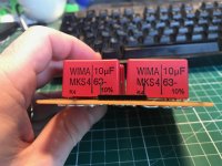
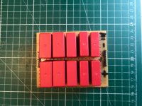
I received yesterday the wima film caps.
My solder lines on the perfboard are really dirty(It is my first use of perfboard).
Please tell me if it is the right way to go or if I am wrong.
After that, I will try your output stage mod.
Attachments

Hi Terry,
Katana won't sound its best IME until powered as I last described with linear supplies and the film caps you have there. Makes a big difference from 2 or 3 SMPS. Katana with SMPS only is inferior and easy to beat. Same goes for any other dac that uses SMPS with only one exception I know of and that is Benchmark DAC-3. For the $2,200 price, they can afford to put a lot of engineering into a combination of preventing and cleaning up SMPS noise. I have never seen it done successfully at lower cost.
Looks like you have soldered the film caps correctly. You should probably practice cleaning up where you got some solder in places where it should not be. I would use Chem-Wik solder wick to clean up and remove excess solder. The most useful size is probably like this: Chemtronics Desoldering Braid, Chem-Wik, Rosin, 10-50L 0.10", 50ft. - Solder Braid - Amazon.com It is a good brand, but in some cases a little extra electronics paste flux can come in handy, especially for difficult solder removal jobs. Amazon.com: MG Chemicals 8341 No Clean Flux Paste, 10 ml Syringe by MG Chemicals: Home Improvement Doesn't take much, use sparingly, or you can clean up with alcohol if necessary. 824-100ML 99.9% Isopropyl Alcohol, 4.2 fl. oz. Bottle: Amazon.com: Home Improvement
The other thing to be aware of is that pre-tinned perfboard is far superior for soldering than the bare copper stuff. I probably should have mentioned that before. Sorry, it didn't even occur to me. I never use the bare copper stuff which is junk in comparison to the tinned/plated type. The better perfboards are usually green color and the holes are plated through the inside for best solder penetration. AUSTOR 100 Pcs PCB Board Kit Including 30 Pcs Double Sided Prototype Boards and 30 Pcs 40 Pin 2.54mm Male and Female Header Connector(Bonus: 10 Pcs 2P&3P Screw Terminal Blocks and 30 Pcs Jumper Caps): Amazon.com: Home Improvement
Last edited:
If source is rpi(1,2,3) no dac will be playing as it can if it will be supplied with better supply.
Hi Terry,
One other thing, from looking again at the picture of your soldering, it is not clear if you used a piece of wire tie adjacent pins together or tried to do it with solder bridges? The correct way would be to lay a long piece of wire along all the holes you want to solder together. Then solder one end, pull it tight and solder the other end or the next corner. Then you can just go down to row soldering all the cap pins in the middle one by one. If you run out of flux trying to heat a joint, or don't use a big enough tip or enough heat then you may get some of the ugly looking Joints like you have in the middle.
You could wick off the bad solder, with or without some added flux, or slowly add a bit more solder which will add some flux and try to get the rough solder to flow into a smoother shape. If it is too hard to heat quickly before the flux burns off, you need a bigger tip and or higher temperature to get the solder flowing and done more quickly.
It is something that takes some practice and experimentation if you are learning alone. If you have someone more experienced to demonstrate learning can go much faster. Youtube videos can help too.
Remember, connections and solder need to be clean for soldering to work properly!!! Oxidized copper or dirty oxidized solder are bad. Clean off the copper with a scouring pad and thoroughly remove any residue of using bare copper perfboard. Gently wipe off solder wire with a folded paper towel or equivalent until all the dark colored junk stops coming off on the paper.
Then try to solder fast, using a big enough tip and enough heat to get in heat, flow solder and get out. They always say to heat the joint then touch the solder to the joint not the iron. Doesn't always work unless the iron tip is freshly cleaned and tinned with solder. Once the flux wears off the tip will be dirty again. It happens in seconds. Soldering is about constantly wiping the tip clean, touching it to a joint, maybe touching a tiny bit of solder to the tip to wet it them quickly move the solder back to the joint.
If you look at the video I posted a long time ago of soldering an SMD IC, you could see it happened very fast. I got the solder flowing, fed it in where I wanted it to go and go out fast. That's the kind of thing to experiment with and practice. Its not perfect work, but if you want to look the link is here: Dropbox - SMD Solder.MOV
You may notice that any solder applied to the tip to wet it tends to flow away from area you are trying to heat to the other side of the tip. That's because solder flows to where there is more heat and that side of the tip isn't being cooled by trying to heat the joint. I compensated for that by rotating the iron in my fingers a little to bring the side of the iron with the solder around in to contact with the joint. Once it wetted the joint, heat transfer improved and solder went where it was supposed go.
Last edited:
Mark,
What clock divider are you using and what ratios do you require?
T
???
I'm thinking divide 100MHz by 4 to get 25MHz. Already have an Arduino program up and running to write SPI. Need to wire it up and test it. Also, thinking about seeing if phasing the AK4137 clock relative to the Q2M clock can help optimize stable DPLL (its easy to do with the divider chip, so may as well see if it can do anything useful). Divider is LMK01000. Numbers like 30fs additive jitter from 100Hz to 20MHz sound pretty good to me. You have something better?
- Home
- Source & Line
- Digital Line Level
- ES9038Q2M Board