I am not alone, some other members have replied to your proposals.It is your selective recitation of facts and refusal to consider or even respond
Facts are intransigent. Current is dependant of voltage and impedance. The impedance of the feedback network has no influence on the current delivered (not entering) by the inverting current. Another mechanism than current has to be resorted to explain the work of feedback in all circonstances. There is necassarily a differential process in a servoing process. In both CFAs and VFAs, a differential device is clearly identified.to others that cements your intransigence.
I'm surprised no one wants to try the design challenge. Use the stock 3904/3906 models that come with LTspice and make a 20dB gain line stage from a 20K pot that drives 600 Ohms at 2V rms. To make it simpler just use 19kHz and 20kHz IMD (2V rms total) as the metric. Maybe set a supply current limit of 10mA and allow ideal sources to set up the bias, but real transistors in the signal path. Tracing out where the distortion comes from is a useful exercise.
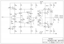
Not exactly what you asked, not CFA as no GNFB used, but CMA, different transistors and more importantly the potentiometer is not at the input, but after Current Conveyor block. In that way noise is almost constant and lower at low volume compared with the potentiometer at the input. This pre amp has quite low distortion too.
Damir
Attachments
The best way to settle this to derive the transfer equation for a CFA without explicitly invoking current flowing through Rf and Rg. If that can be done, a CFA is a VFA in my book.
The derivation must apply from DC to HF.
The derivation must apply from DC to HF.
I am not alone, some other members have replied to your proposals.
Yes, and they agreed with them! They just thought that they were irrelevant - irrelevant only because they don't agree that the CFA operates with voltage feedback. Which was the point of the Post - it is relevant to those who believe that it does.
The circuit itself is called a CFA, no matter what connections are made.Thanks for following through on my query in Post 1321 for Rf very large or the case of no Rf.
But doesn't your open loop test bring an apparent contradiction with it? How can you say you have a CFA when there is no feedback in open loop? Wouldn't it then be just a CA😀?
Or could it be that even in open loop it is still a CFA with current feedback active?😕
Whether it still behaves like a CFA under all conditions is a different questionmark.
Let me try to explain what happens with a CFA with only Rg connected.I suggested that there is still current feedback in open loop as emitter degeneration of the input stage. Your voltage gain plots show about 48dB difference between them and assuming this is due to degeneration feedback in the input stage then we can calculate the Rn or 1/gm as 12k5/250 (from 48dB) or Rn~50 ohms and is in the right ball-park of 25-50 ohms. That supports the idea that the 12k5 gives 48dB of degenerative feedback to the input stage in this open loop test.
Then, if Rf is reintroduced, you get current fed into the emitter resistor that relieves the input transistor of current since there is a lot of current gain in the output buffer (~10,000 times). Reducing Rf to a small value (say Rg or less) then most of the feedback current into the emitter resistor comes from the output buffer with only 1/10,000th of the current needed from the input transistor. This can explain current feedback in a CFA at DC and LF..
At the -Input, you will get the same voltage as on the +Input, so far hardly a difference when compared to a situation where Rf is connected.
But the big difference now is that not the output is supplying the current through Rf, but the full current to Rg has now to come now from In-.
Let's call this current X. Through the current mirror inside the CFA this current is transferred to Z(s), resulting in an output voltage of X*Z(s).
The LF part of Z(s) is resistive, so when seeing a 20dB gain with Rg of 12k5, this means that this Z(s) is 125K.
Looking at the tranfer curve, we see a -3dB point at 375Khz.
Conclusion is that Z(s) is ca 125K//3pF.
Below I have added an image made with 3 different values for Rg, lying 10dB apart.
What you can see is that V(out) also changes by 10dB, but the open-loop calculation stays the same somewhat below 70dB.
With a buffered CFA this behaviour with Rg is absolutely not the case, that's why it is a VFA as also came out clearly from the DIT.But what about VFA's including H-bridge or buffered CFA's (which are VFA's)?
I think the Middlebrook/Franco observation that you have a CFA when there is enough degeneration of the input stage with a tipping point at 3dB of degenerative current feedback in the input stage, and then a factor of 10 (or 20dB) to be clear of the transition region where we have a mix of both.
Hans
Attachments

You can also reason that for a CFA without Rf, but with Rg, that input stage acts like an emitter follower and we all know emitter followers have 100% current feedback 😎
This is also true with Rf connected. The current from Rg then reduces the load seen by the input emitter whose current is considerably reduced. The ultimate form of this is when Rg equals 0 Ohm and is illustrated by the Sziklai complementary pair.You can also reason that for a CFA without Rf, but with Rg, that input stage acts like an emitter follower and we all know emitter followers have 100% current feedback 😎
In an emitter follower (remember 100% feedback), the emitter is a voltage input, not a current input.
the emitter is a voltage input, not a current input.
Not according to Post 1028.
For my own amusement, i have been interested in low to moderate OLG circuits which are inherently linear as a starting point for audio.
THx-RNMarsh
To expand upon your point lets consider a a standard CFA under open loop conditions having a 3M Ohm resistor at the Tz node. This is the case of an AD844. For a +/- 1.5 volt full scale output (approx. 1 V RMS) the current becomes approx. 0.5uA for full scale into the 3 M Ohm. If we now dare to resolve a 24 bit digital signal the least significant bit current becomes 30 femto amps. This signal is in comparison to the minimal current noise generated by a 3 M Ohm resistor.
This suggests that there exists some form of exponential deterioration of signal to noise ratio with increasing Tz node resistance, given that increasing resistance increases current noise in the resistor, being in combination with decreasing signal currents as necessary to cause the 1 V RMS output. What seems even worse is that a Tz node resistance of 3 Meg Ohm becomes an antennae for the power supplies that need only inject 30 femto amps to disturb the device.
If the object is for audio purposes this doesn't seem the way to go, rather to be avoided. It seems these devices would be vastly improved by cutting down on the open loop gain, as potentially why discreet networks are often used in lieu of them in high end audio.
To expand upon your point
If the object is for audio purposes this doesn't seem the way to go, rather to be avoided. It seems these devices would be vastly improved by cutting down on the open loop gain, as potentially why discreet networks are often used in lieu of them in high end audio.
🙂 😎
-RNM
Reduced to the point where this current I(in-) causes an output voltage V(out) = V(in+)+I(in-)* Z(s) is where I(Rf) + I(In-) = I(Rg) or V(out)/V(In+) = 1+ Rf/Rg, neglecting a tiny little difference depending on loop-gain.This is also true with Rf connected. The current from Rg then reduces the load seen by the input emitter whose current is considerably reduced.
As you can see in the third formula above, when Rg=0, V(out) becomes 1+Rf/0 =1+infinite and the CFA stops functioning !The ultimate form of this is when Rg equals 0 Ohm and is illustrated by the Sziklai complementary pair.
No idea what you mean by this. Vbe is a voltage input, but the relation between Vbe, Ic, and Ie is basically through current and not voltage, even for an emitter follower.In an emitter follower (remember 100% feedback), the emitter is a voltage input, not a current input.
Only when an emitter follower has a perfect current source on its emitter, you might come close to 100% feedback, but for a CFA -Input this is not the case.
Hans
DIT test conundrum
But your DIT jig (post 1276) can show the LT1395 CFA can be made to look like a VFA by setting R2 to say 10 ohms. The circuit is attached.
When you change R2 (back) to 1k, it becomes a CFA by the DIT test (blue line for I ratio now below the V ratio). The change is simply a lower resistances in the feedback. Same topology.
For a buffered CFA, which is said to become a VFA, it too can be morphed back into a CFA if the resistors Rf//Rg is set high enough. Take a single transistor buffer on the inverting input of a CFA (like the LTP). The tip point from VFA/CFA is when
Rf//Rg ~ 2/gm*Beta . E.g. 1mA, Beta=100 then
Rf//Rg ~ 2*25R*100 or 5k ohms. So Rf//Rg >>5k your buffered CFA is back to a CFA by the DIT test.
For a diamond buffered CFA there are two beta's (effectively 4 Vbe's in series) so
Rf//Rg ~ 4/gm*Beta*Beta or 100R*100*100 or 1Meg. So Rf//Rg >>1Meg your diamond buffered CFA (datasheets call this a VFA) is back to a CFA by the DIT test.
So under the DIT test method you cannot have topology specific to the CFA and another topology specific to the VFA, since under the DIT test you can morph one to the other simply by choosing different resistors in the feedback loop. That is our conundrum.
Can I assume you are saying a CFA is by definition a topology?The circuit itself is called a CFA, no matter what connections are made.
Whether it still behaves like a CFA under all conditions is a different questionmark.
But your DIT jig (post 1276) can show the LT1395 CFA can be made to look like a VFA by setting R2 to say 10 ohms. The circuit is attached.
When you change R2 (back) to 1k, it becomes a CFA by the DIT test (blue line for I ratio now below the V ratio). The change is simply a lower resistances in the feedback. Same topology.
For a buffered CFA, which is said to become a VFA, it too can be morphed back into a CFA if the resistors Rf//Rg is set high enough. Take a single transistor buffer on the inverting input of a CFA (like the LTP). The tip point from VFA/CFA is when
Rf//Rg ~ 2/gm*Beta . E.g. 1mA, Beta=100 then
Rf//Rg ~ 2*25R*100 or 5k ohms. So Rf//Rg >>5k your buffered CFA is back to a CFA by the DIT test.
For a diamond buffered CFA there are two beta's (effectively 4 Vbe's in series) so
Rf//Rg ~ 4/gm*Beta*Beta or 100R*100*100 or 1Meg. So Rf//Rg >>1Meg your diamond buffered CFA (datasheets call this a VFA) is back to a CFA by the DIT test.
So under the DIT test method you cannot have topology specific to the CFA and another topology specific to the VFA, since under the DIT test you can morph one to the other simply by choosing different resistors in the feedback loop. That is our conundrum.
Attachments
A transistor can be seen as having two main correlated functions.Originally Posted by forr
In an emitter follower (remember 100% feedback), the emitter is a voltage input, not a current input.
No idea what you mean by this. Vbe is a voltage input, but the relation between Vbe, Ic, and Ie is basically through current and not voltage, even for an emitter follower.Hans

- the current circulating across it is under the control of Vbe which is the difference of voltages between its base and its emitter .
- the voltage of its emitter replicates the variations of its base voltage.
I am not aware that, for an emitter follower, the vertue of following applies to anything else than voltages.
A transistor is a differential input device and has an analogy with an op-amp (see my post #1121). The differential operation is only be possible with values of same nature (that's the big incoherence of the CFA naming).
As a consequence, it is perfectly legitimate to qualify the emitter as a voltage input.
The emitter also delivers current from a low impedance source.
So the emitter combines two sub-functions, delivering current and sensing voltage at once.
The 100% feedback of an emitter follower is an affair of voltages.
Hierfi,
An explicit account of VFA and CFA can be given, but not within Control Theory. There is much more to it than Ohm's law can tell.
The other way around. Representational terms must bear reference to static (invariant) states, they become nonsensical when applied to signals. Some inferences can be made as a purely mental model, but, yes, it is targeting an imponderable, unimaginable complexity. Truth is a wrong word for the context.
Because ultimately signal distortion that matters.
Well said.
Is it generally held that no-one can figure out the characteristic behaviour of a VFA or CFA under DC conditions?
Is it taken for granted that under DC conditions these devices can't be characterized as VFA's or CFA's?
An explicit account of VFA and CFA can be given, but not within Control Theory. There is much more to it than Ohm's law can tell.
Is it that truth can only be derived from the seemingly extremely more complex behaviour under AC conditions?
The other way around. Representational terms must bear reference to static (invariant) states, they become nonsensical when applied to signals. Some inferences can be made as a purely mental model, but, yes, it is targeting an imponderable, unimaginable complexity. Truth is a wrong word for the context.
The point is why is anyone bothering with AC artifacts
Because ultimately signal distortion that matters.
If the object is for audio purposes this doesn't seem the way to go, rather to be avoided. It seems these devices would be vastly improved by cutting down on the open loop gain, as potentially why discreet networks are often used in lieu of them in high end audio.
Well said.
SPICE BJT model accuracy
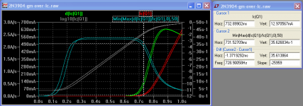
Attached is a jig that plots a 2N2904 with swept Vbe. It includes a plot of Gm/Ic which is constant over 7 decades of Ic. Gm/Ic is in Siemens per Ampere or ~40 mA/V per mA at 20C.
The first attached plot shows the Gm/Ic ratio degrades by 10% when Ic~13mA
The second attached plot shows Gm/Ic with Vce stepped 1V 10V and 100V. Notice there is no effect on the Gm/Ic ratio in the middle region..
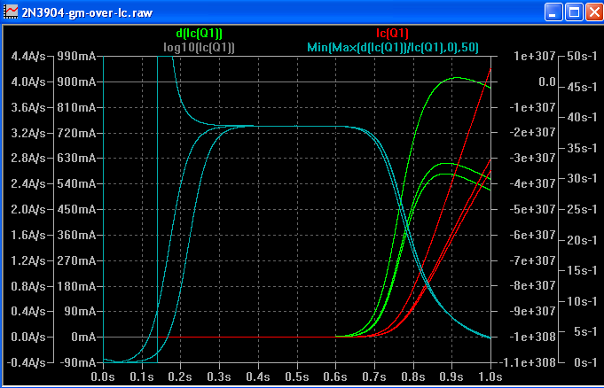
You can step Tj, or Re by uncommenting the unused .Step lines.
Sorry I took so long to get around to this.
Cheers,
IH
Hi Chris,...My claim refers to the relative importance of two mechanisms in the input transistors: Early and transconductance.
....
Finally, if the transistor spice models are not to be accepted as reasonably accurate in this sense, then we shouldn't waste our time with any transistor simulations.
Attached is a jig that plots a 2N2904 with swept Vbe. It includes a plot of Gm/Ic which is constant over 7 decades of Ic. Gm/Ic is in Siemens per Ampere or ~40 mA/V per mA at 20C.
The first attached plot shows the Gm/Ic ratio degrades by 10% when Ic~13mA
The second attached plot shows Gm/Ic with Vce stepped 1V 10V and 100V. Notice there is no effect on the Gm/Ic ratio in the middle region..
You can step Tj, or Re by uncommenting the unused .Step lines.
Sorry I took so long to get around to this.
Cheers,
IH
Attachments

Last edited:
Scott,
Further to your Challenge, I have made two different models.
One is based on the Classical long tail topology and the other one on a buffered CFA, thus also being a VFA.
It appears that the classical version is better in all aspects, Noise, Slew Rate and IMD, see table below.
To separate both in the table, one is called VFA and the other one CFA, but they are of course both VFA's.
To prevent too much gain, only R3 is now representing the 20k pot.
Gain can be set from 0 to 10x.
For both cases supply current is just below 10mA.
It is of course possible to change both in a non inverting amps, but input capacitance will then start playing a role when steered from a 20k pot.
Hans
Attachments


Hi Chris,
Attached is a jig that plots a 2N2904 with swept Vbe. It includes a plot of Gm/Ic which is constant over 7 decades of Ic. Gm/Ic is in Siemens per Ampere or ~40 mA/V per mA at 20C.
Hi Ian,
This is to be expected. It is something I have never addressed and certainly never contested.
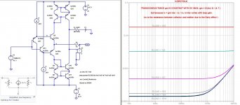
Please take a look at the tremendous variation in ic /vbe in the attached CFA as we vary the loop gain by changing R_LOAD. (Thanks to Scott Wurcer, whose .asc file of an AD844 I borrowed and modified.)
Certainly the DC operating conditions aren't changing; gm = 1mA q / (k T) for all gains. So why does ic / vbe change so much?
The reason is as follows. the collector current consists of a transconductive current (gm vbe ) minus a resistive current (vce / ro). vbe is driven lower as loop gain increases, but vce remains constant. For adequately high gains, the magnitudes of the transconductive and resistive currents are almost identical, with the former being slightly higher to provide the necessary current to drive the circuit. Further increases in gain would not make much difference in the magnitude of either. Q6 could swapped with its Hybrid Pi model and both currents tracked independently so that you could see this in more detail. This is what I have been trying repeatedly without success to get forr to acknowledge.
You'll need to change the attached .txt file to .inc to run this simulation.
Attachments
Are you sure about your emitter follower theory ?A transistor can be seen as having two main correlated functions.
- the current circulating across it is under the control of Vbe which is the difference of voltages between its base and its emitter .
- the voltage of its emitter replicates the variations of its base voltage.
I am not aware that, for an emitter follower, the vertue of following applies to anything else than voltages.
A transistor is a differential input device and has an analogy with an op-amp (see my post #1121). The differential operation is only be possible with values of same nature (that's the big incoherence of the CFA naming).
As a consequence, it is perfectly legitimate to qualify the emitter as a voltage input.
The emitter also delivers current from a low impedance source.
So the emitter combines two sub-functions, delivering current and sensing voltage at once.
The 100% feedback of an emitter follower is an affair of voltages.
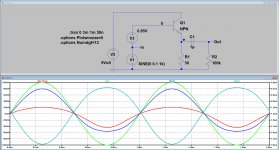
See image below with:
Input voltage: Green
Output voltage: Blue
(Input Voltage)-(Output Voltage), that according to you should be constant: Red
Emitter Current: Cyan.
Attachments
Scott,
Further to your Challenge, I have made two different models.
One is based on the Classical long tail topology and the other one on a buffered CFA, thus also being a VFA.
It appears that the classical version is better in all aspects, Noise, Slew Rate and IMD, see table below.
Hans
Interesting, I wonder if you would get these sub-ppm distortions in real life.
The emitter follower reduces the cause effect issue to the simplest case. The voltage and current have a very basic relationship and they are not independent. Force current back into it and the voltage changes.
Last edited:
It's a way to see things.Are you sure about your emitter follower theory ?
I usually avoid to make transistors working with such a non linearity.See image below with:
Please again, do not twist my words.(Input Voltage)-(Output Voltage), that according to you should be constant: Red Emitter Current
- Home
- Amplifiers
- Solid State
- Current Feedback Amplifiers, not only a semantic problem?