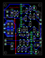
Is this better?Upupa Epops said:I guess that this design of PCB is not good and will bring problems with hum, 'cos ground loop is closed. It must be interrupted and ground of both channels must lead to the middle of PS separately.
Attachments
tcpip said:
Is this better?
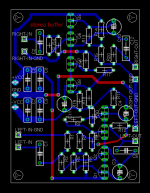
Great layout Tarun, you are a pro already. There are just these 2 things I would do.
1. Put the powersupply ground jumper directly at the output gnd instead of Right input gnd as you have done.
2. Avoid taking tracks from inbetween TO92 pads, use a jumper, or you can reorient R4. It will give you much less problems later.
Angshu
PCB
Hi tcpip : This is better, but try it redesign - if you get PS to the oposite side of PCB ( between outputs ), result will be much more elegant and " electricaly " correct 🙂 .
Hi tcpip : This is better, but try it redesign - if you get PS to the oposite side of PCB ( between outputs ), result will be much more elegant and " electricaly " correct 🙂 .
Re: Re: Re: Some general doubts about layout and component placement
Resistors are usually mounted horizontally because vertical mounting makes the board difficult to service (probing and component removal are difficult). Other reasons include reduced profile and suitability to pick-and-place machines.
Grounds are kept seperate only to prevent large currents which can share a ground line from interfereing with smaller currents which also flow in that line. If your circuit has an amplifier, then it's power supply will have transients when the output varies. This should not couple back in, why we seperate the traces. Now the coupling can also happen if the supply decoupling capacitors are allowed to connect to a ground path near the signal ground. So lump together the amp's power ground (if any) and decoupling cap ground, return these to a low impedance point seperately (need not always be the supply, if local decoupling to a stable ground is available, that will do). The output return should go back to ground seperately, as should the input ground. The input ground also includes the amplifier's reference point (for eg the opamp + terminal in an inverting amp). This will, in general, avoid a great deal of trouble with grounding. Analog Devices AN-202 explains this better than most other places.
As for the last point, you have to figure out what the reference for the signals are and connect the shield there. Otherwise, the noise present between the signal reference and the shield will couple capacitively into the signal flowing in the centre conductor.
tcpip said:Ok, here are some general questions:
Thanks,
- Why don't any PCBs I see have vertically mounted resistors? I'm talking audio frequencies, not frequencies where every wire acts like an antenna. Won't vertical resistors save a lot of space?
- What are your thoughts about how to do layout ground tracks for audio preamp-type circuits? Is a star ground needed? Is it necessary to keep signal ground separate from supply ground? Which of the following do you do?
(i) Keep the two totally separate; join them outside the board at some star ground point
(ii) Keep them separate for the entire board, except at one "star" point where you join them (that's what I've done in the board above)
(iii) join them freely wherever you feel like, because the magnitudes of current flowing through these tracks is so minor anyway.- When you take shielded hookup wire from PCB to pots/switches, where do you ground the shield? Do you make a ground solder-pad on the PCB for the shield of each such cable? If not, what else?
Tarun
Resistors are usually mounted horizontally because vertical mounting makes the board difficult to service (probing and component removal are difficult). Other reasons include reduced profile and suitability to pick-and-place machines.
Grounds are kept seperate only to prevent large currents which can share a ground line from interfereing with smaller currents which also flow in that line. If your circuit has an amplifier, then it's power supply will have transients when the output varies. This should not couple back in, why we seperate the traces. Now the coupling can also happen if the supply decoupling capacitors are allowed to connect to a ground path near the signal ground. So lump together the amp's power ground (if any) and decoupling cap ground, return these to a low impedance point seperately (need not always be the supply, if local decoupling to a stable ground is available, that will do). The output return should go back to ground seperately, as should the input ground. The input ground also includes the amplifier's reference point (for eg the opamp + terminal in an inverting amp). This will, in general, avoid a great deal of trouble with grounding. Analog Devices AN-202 explains this better than most other places.
As for the last point, you have to figure out what the reference for the signals are and connect the shield there. Otherwise, the noise present between the signal reference and the shield will couple capacitively into the signal flowing in the centre conductor.
Aapki kripa, Gurudev.angshudas said:Great layout Tarun, you are a pro already.
Done1. Put the powersupply ground jumper directly at the output gnd instead of Right input gnd as you have done.
Done again. How does this one look? Are the jumpers okay?2. Avoid taking tracks from inbetween TO92 pads, use a jumper, or you can reorient R4. It will give you much less problems later.
Attachments
Did you build this buffer
Hello Tarun,
Did you build this buffer? If so, how does it sound. Please share your results with us.
Thanks,
Routhun
Hello Tarun,
Did you build this buffer? If so, how does it sound. Please share your results with us.
Thanks,
Routhun
Re: Did you build this buffer
routhun The Latest schematic posted here, is from February of 2004. (3.5 years ago)
I have seen tcpip around. He is from India. In my folder on him, I can see he posted his own version of Randy Slone blameless power amp in January 2007.
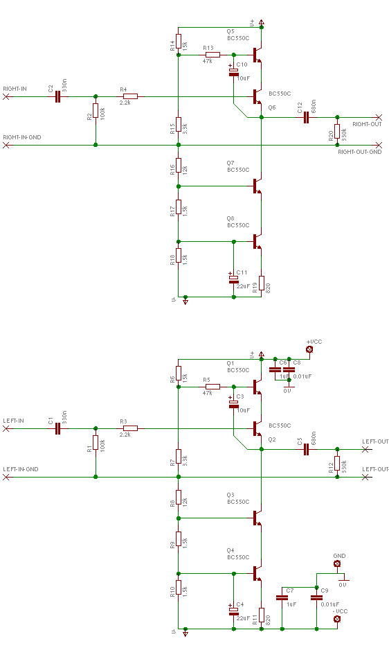
So, he might, if he notice your post, tell you the story of this preamp buffer based on 4 low noise BC550C transistors
See my attached schematic 😎
Idea of This Circuit: -------------------------------------------------------------------------------------- Normally we can use a bottom current source and an uppper NPN follower as Buffer. And already this give mostly great performance!
Now this circuit takes it One Step further in prefection. Both the CSS and the upper follower BC550C are Cascoded. This means BOTH these transistors, see a constant C-E voltage. And so linearity should be improved by a level = lower distortion. --------------------------------------------------------------------------------------
It is interesting to see two very experienced audio guys jean-paul & Upupa Epops have been positviely interested in this project 😉 jean-paul is a guy, that talk not too much .. but he knows what he talks about, the few times he opens his mouth a little. Upupa Epops is one of the most critical members you can imagine. He can find something 'not right' where all we other miss it. If he is positive 😀 we can assume we are 'close to the sun' in ultimate amplifier --------------------------------------------------------------------------------------
The attached circuit is from Eagle ZIP in Post #86. You should read jean-paul comments in those posts following to get eventual changes needed. Post #86: Simple discrete unity gain buffer - Page 9 - diyAudio
ZIP has got: - disreshun.brd (PCB) - disreshun.sch (Schema) http://www.diyaudio.com/forums/attachment.php?postid=320241&stamp=1076131619
🙂 I think this buffer would be as close to 'the perfect preamp buffer' you can get by using only 4 good low-noise transistors. ( Our alternative: Expensive OP-Amps, having usually 30-50 semiconductors, transistors! )
This is Probably in most applications A Real OverKill Circuit, because already 1-2 Transistors will do very well as buffer / follower, if setup in a good way.
Regards lineup 500 Internal Server Error 🙂
Originally posted by angshudas Great layout Tarun, you are a pro already. There are just these 2 things I would do.
1. Put the power supply ground jumper directly at the output gnd instead of Right input gnd as you have done.
2. Avoid taking tracks from inbetween TO92 pads, use a jumper, or you can reorient R4. It will give you much less problems later.
Angshu
Originally posted by Upupa Epops Hi tcpip : This is better, but try it redesign - if you get PS to the oposite side of PCB ( between outputs ), result will be much more elegant and " electricaly " correct 🙂 .
Originally posted by routhun Hello Tarun,
Did you build this buffer? If so, how does it sound. Please share your results with us.
Thanks, Routhun
routhun The Latest schematic posted here, is from February of 2004. (3.5 years ago)
I have seen tcpip around. He is from India. In my folder on him, I can see he posted his own version of Randy Slone blameless power amp in January 2007.
So, he might, if he notice your post, tell you the story of this preamp buffer based on 4 low noise BC550C transistors
See my attached schematic 😎
Idea of This Circuit: -------------------------------------------------------------------------------------- Normally we can use a bottom current source and an uppper NPN follower as Buffer. And already this give mostly great performance!
Now this circuit takes it One Step further in prefection. Both the CSS and the upper follower BC550C are Cascoded. This means BOTH these transistors, see a constant C-E voltage. And so linearity should be improved by a level = lower distortion. --------------------------------------------------------------------------------------
It is interesting to see two very experienced audio guys jean-paul & Upupa Epops have been positviely interested in this project 😉 jean-paul is a guy, that talk not too much .. but he knows what he talks about, the few times he opens his mouth a little. Upupa Epops is one of the most critical members you can imagine. He can find something 'not right' where all we other miss it. If he is positive 😀 we can assume we are 'close to the sun' in ultimate amplifier
-------------------------------------------------------------------------------------- The attached circuit is from Eagle ZIP in Post #86. You should read jean-paul comments in those posts following to get eventual changes needed. Post #86: Simple discrete unity gain buffer - Page 9 - diyAudio
ZIP has got: - disreshun.brd (PCB) - disreshun.sch (Schema) http://www.diyaudio.com/forums/attachment.php?postid=320241&stamp=1076131619
🙂 I think this buffer would be as close to 'the perfect preamp buffer' you can get by using only 4 good low-noise transistors. ( Our alternative: Expensive OP-Amps, having usually 30-50 semiconductors, transistors! )
This is Probably in most applications A Real OverKill Circuit, because already 1-2 Transistors will do very well as buffer / follower, if setup in a good way.
Regards lineup 500 Internal Server Error 🙂
Attachments
Hi Lineup,
Thanks for the quick reply. I want to use discrete buffer in my preamp. I want to have some gain (around 4~5 is good enough). How can I achieve this? A non-inverting opAmp stage with 4~5 gain before this buffer is good? Can I acheive similar gain with a single FET befor this buffer?
Thanks,
Routhun
Thanks for the quick reply. I want to use discrete buffer in my preamp. I want to have some gain (around 4~5 is good enough). How can I achieve this? A non-inverting opAmp stage with 4~5 gain before this buffer is good? Can I acheive similar gain with a single FET befor this buffer?
Thanks,
Routhun
Originally posted by routhun Hi Lineup,
Thanks for the quick reply. - I want to use discrete buffer in my preamp. - I want to have some gain (around 4~5 is good enough). - How can I achieve this? - A non-inverting opAmp stage with 4~5 gain before this buffer is good? - Can I acheive similar gain with a single FET before this buffer?
Thanks,
Routhun
Yes, you can try out that 'Our FET Master' Nelson just posted: JFET BOZ It will work good = give good sound, otherwise he wouldnt put it on public. It does not cost much, but be sure to make a good Power supply for that JFET amp.
To have at home, a private storage, for Quickly Build Good Custom PSU, power supply, is good: ---- with 10-25 LM317T and a bunch of 5-10VA small transformers plus maybe 10-20 pieces of 'Adjustable Precision Shunt Regulator - TL431' TL431 2% Accuracy Adjustable Precision Shunt Regulator | TI.com
20 x Red 5mm LEDs, to use for 1.60 Volt Reference, and in CCS, constant current sources. I can also recommend BF245A / BF245B, low price JFET, for use as 'stand alone' CCS. Philips: N-channel FET|NXP
==============================================================
Buffers are often good use in pre amplifier lines, whether they are 1,2,3 or 4 transistors, bipolar BC550C or JFET 2SK170 etc. ----------------------------
1. buffers can be put before and after a Volume Pot to keep the fequency behavior (audio bandwidth) constant when the resistance of pot is changing
2. buffers can 'take the load way' from a voltage amplifier if used as a buffer at the output
3. the less the load, the less distortion in voltage amplifier
4. voltage amplifier stage, transistor is when INPUT is at BASE and OUTPUT is at COLLECTOR ( gate-drain for FET )
5. buffer, follower is INPUT BASE and OUTPUT EMITTER ( gate-source for JFET) ----------------------------
So what is the Hook here?
Yes, the behavior of a transistor, when input at BASE and output at COLLECTOR is very much different from the other case, input BASE and output EMITTER.
The term itself tells it: Follower which means Input voltage = Output voltage .... (almost, just a little bit less)
When output is taken from collector, the result is not as straight. We can say it is less linear, and also the HEAVIER the LOAD is, the less linear those curves will be.
Have a look at some linear and less linear (more bending) curves in this datasheet of a bipolar transistor, BC550C This is Datasheet, that all we diy audio people HAVE to study! Many amp designers knows these curves in their head .. by heart .. at their fingertips.
Not Found - Datasheet Archive
============================================= some other useful links, that pops into my mind here:
1. TalkTalk Webspace is closing soon!! DESIGN WITH DISCRETE TRANSISTORS Very good! With some examples how transistor can be used.
2. TalkTalk Webspace is closing soon!! Distortion in Power Amplifiers. Lots of interesting figures/images. The best & most complete publicly FREE work, so far, in this art of making (Power) Amplifiers.
2. http://www.passdiy.com/legacy.htm ... look for D.I.Y. Op Amps: by Nelson Pass An Essential Reading and looking! Circuit suggestions.
3. http://sound.westhost.com/no-opamps.htm Opamp Alternatives (= Transistors!) - A sample of the circuits that were in common use before opamps 'took over'
4. http://sound.westhost.com/site-map.htm ... look for anything! like: - Class- A - a discussion of the benefits of Class-A amplifiers - More Truth About Cables - Amplifier Basics - How Amps Work - Amplifier Design With HEXFETs - Noise in Audio Amplifiers - Transistor Matching Tests - Power Supply Design - How to design linear power supplies - transformers, rectifiers and filters
=============================================
As you see - only 3 websites, and besides www.diyaudio.com these 3 make up so much good information, that anyone into making transistors work good, should defintitely not miss those 😉
It will also help for to follow the discussion here. As these are Refered To in DIYaudio world .. and they are good starting points .. for later takings things much further, if possible
Regards lineup 🙂
Made a low voltage buffer with a depletion mode fet (bsp135 if I remeber correctly) just the fet and a resistor.. That worked nicely but it wasnt hifi-critical at that point.. If I'd do it now I'd try maybe irf610 and 9610 in some kind of diamond complementary design or whatever it's called.. (I made such a thing, but had no use for it so i dont know irl how it would sound, only through the function generator and scope, and spice of course it was nice..
routhun said:Thanks lineup for the JFET BOZ.
Routhun
🙂 thanks for your thank
and .. no problem, because:
😉 this is what I am here for, routhun
* here - in exsistense, in life, living for
... a social animal lives not solo
... a social human will support others,
... his 'friends'
... his social group & so, his Own environment of Living & survival
lineup

i p2p'd this and it sounds marvelous. probably the best i've heard for the parts count that it has. is 10uf the positive feedback? and can i increase it for more bass?
so once again, its this circuit
how can i bias this higher? do i change the bottom resistor 1.5k ohm and the top resistor 15k to lower values?
and is the input resistor necessary if you're not putting a pot before it?
how can i bias this higher? do i change the bottom resistor 1.5k ohm and the top resistor 15k to lower values?
and is the input resistor necessary if you're not putting a pot before it?
Most SE Class A amps will have a turn on thump. There are a few ways to prevent it. 1) use a cap multiplier on the supply to slowly ramp up the voltage over 10seconds. Something like this (has a 4v dropout penalty though); 2) use a relay with time delay circuit either RC constant or microcontroller.
Xr971, i do use that cX, but mine the voltage comes up rather fast?
Ah so the buffers class a. No wonder i like the sound so much. Do u perhaps have any other 0gain circuits i can compare to?
Ah so the buffers class a. No wonder i like the sound so much. Do u perhaps have any other 0gain circuits i can compare to?
- Status
- Not open for further replies.
- Home
- Source & Line
- Analog Line Level
- Simple discrete unity gain buffer