Are you suggesting converting the amplifier into a balanced input drive?
You can find the answer in the first sentence of his post (#79).
Tom
I would strongly suggest to balance or minimize impedances next to the first opamp inputs
Does this mean using for example, 100R vs 2k2 on input?
Minimize = make as small as possible.
Balance = make equal.
Balancing the impedances on the two inputs of an opamp is commonly done to improve CMRR and to compensate for DC offsets caused by the input bias current. In case of the OPA1688, it sounds like it has other advantages as well.
You can see Chapter 5 of Sergio Franco: “Design with Operational Amplifiers and Analog Integrated Circuits”, McGraw-Hill, 2002, ISBN: 0-07-232084-2 for examples. I'm sure it's covered in Walt Jung's book as well.
Tom
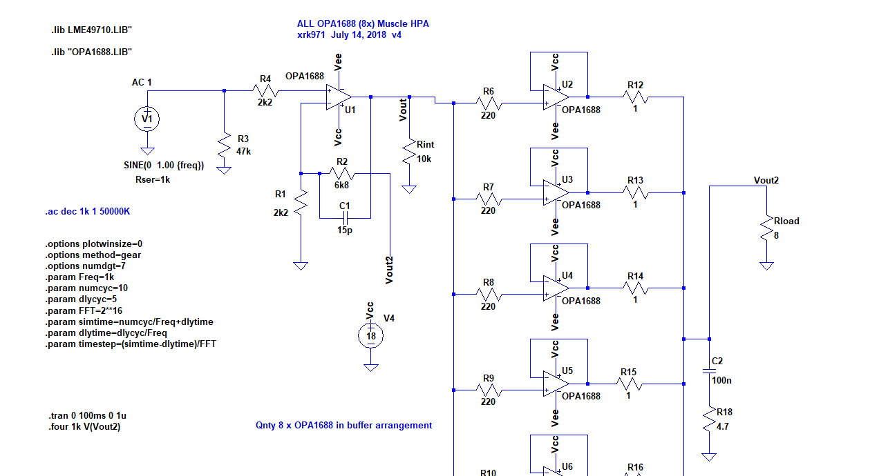
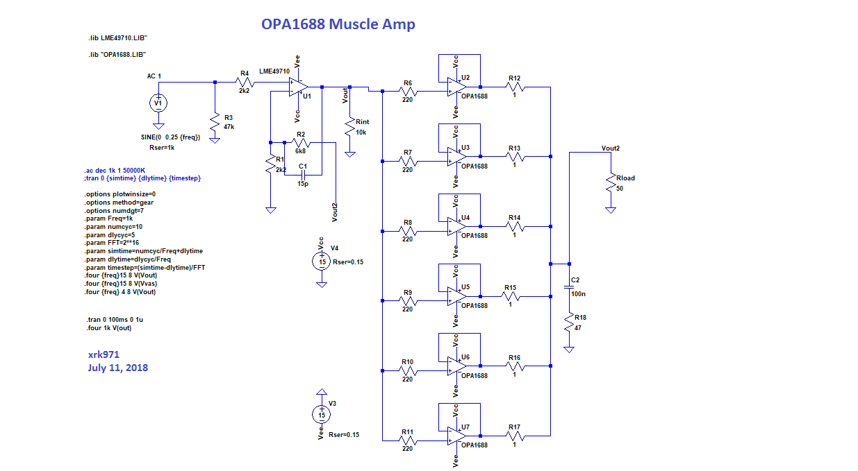
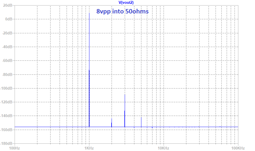
If I did this right, the 2k2 (R1) and 6k8 (R2) presents a 1660R impedance to the negative input, so we need to match this impedance on the positive input. However, when accounting for the 47k (R3) to ground, a value of 1720R for R4 is needed to present a 1660R impedance to the positive inout. The sim result was unchanged. I tried minimizing the impedance by making the feedback 680R and the ground shunt 220R, this effectively makes the 47k unimportant and a 166R R4 was used. The sim for this actually showed distortion increasing from 0.000063% to 0.000068%. Doing this also makes the output effectively driving a 166R load under full power - quite a bit of dissipation and a much larger power resistor would be needed. I think I will keep it at 6k8 and 2k2 with 1720R R4.
Last edited:
The sim for this actually showed distortion [...]
...which still isn't covered by the model. Neither is the effect Shaq888 pointed out.
Best of luck with your amp. I hope we get to see measured results from it one of these days.
Tom
Just to demonstrate how detached from the reality those distortion simulations are.
I took your schematic from the first post
and optimized thevalues. Also I used only 4 opamp in parallel at the output (which should not work in my favor...)
...and I'm getting distortion plots like this for 3Vrms, which is pretty much 8.5Vpp on 45Ohm load (plot is in dBc)

instead of what you were showing there before:
Do you still think any of those models can give realistic THD simulations?
I took your schematic from the first post
and optimized thevalues. Also I used only 4 opamp in parallel at the output (which should not work in my favor...)
...and I'm getting distortion plots like this for 3Vrms, which is pretty much 8.5Vpp on 45Ohm load (plot is in dBc)
instead of what you were showing there before:
Do you still think any of those models can give realistic THD simulations?
@xrk: consider this post: New Audio Op Amp - OPA1622 It was posted by an engineer from TI.
You might want to read this to: https://www.google.be/url?sa=t&sour...FjAAegQIBBAB&usg=AOvVaw0_E42s6t4A0p1HfxpXXTvs
The opa1688 isn't doing too bad but you might consider a opa1642 as input opamp.
BTW, perfect balancing of impedance is impossible after a pot (it is a varying source impedance). So you have to take into account is maximum impedance, to minimize distortion when its impact is at its worst.
Last edited:

Rule breaking and insulting posts have been deleted. Don't let what appears to be an interesting thread descend into one of trading insults. Argue your points on technical grounds.
Yeah, tracking supply rails or floating cascode with external BJT pair would double the complexity.
Also inverting configuration + linear pot can create almost like logarithmic characteristic, but that puts a bit of a current load on a wiper.
Also inverting configuration + linear pot can create almost like logarithmic characteristic, but that puts a bit of a current load on a wiper.
Last edited:
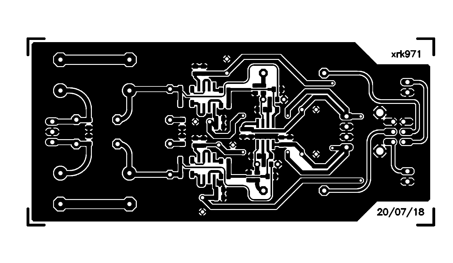
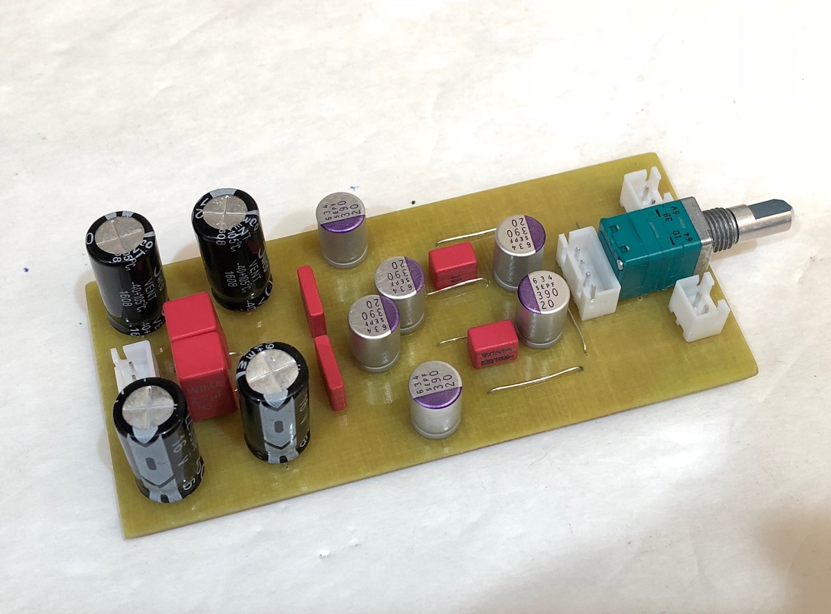
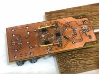
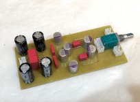
Here is a DIY'able single-layer board layout for a pair of paralleled buffers in SOIC8 that JPS64 made. It includes some nice low ESR caps (390uF 20v OSCON + 10uF X7R + 0.1uF X7R for both rails at the power supply pins) and also the option to cap-couple the input or output.
Schematic (note, for balanced opamp inputs (w/ pot at full volume) use R104 & R105 = 1.72k, and R111 & R112 should be high quality metal thin film, or carbon film, but not thick film):
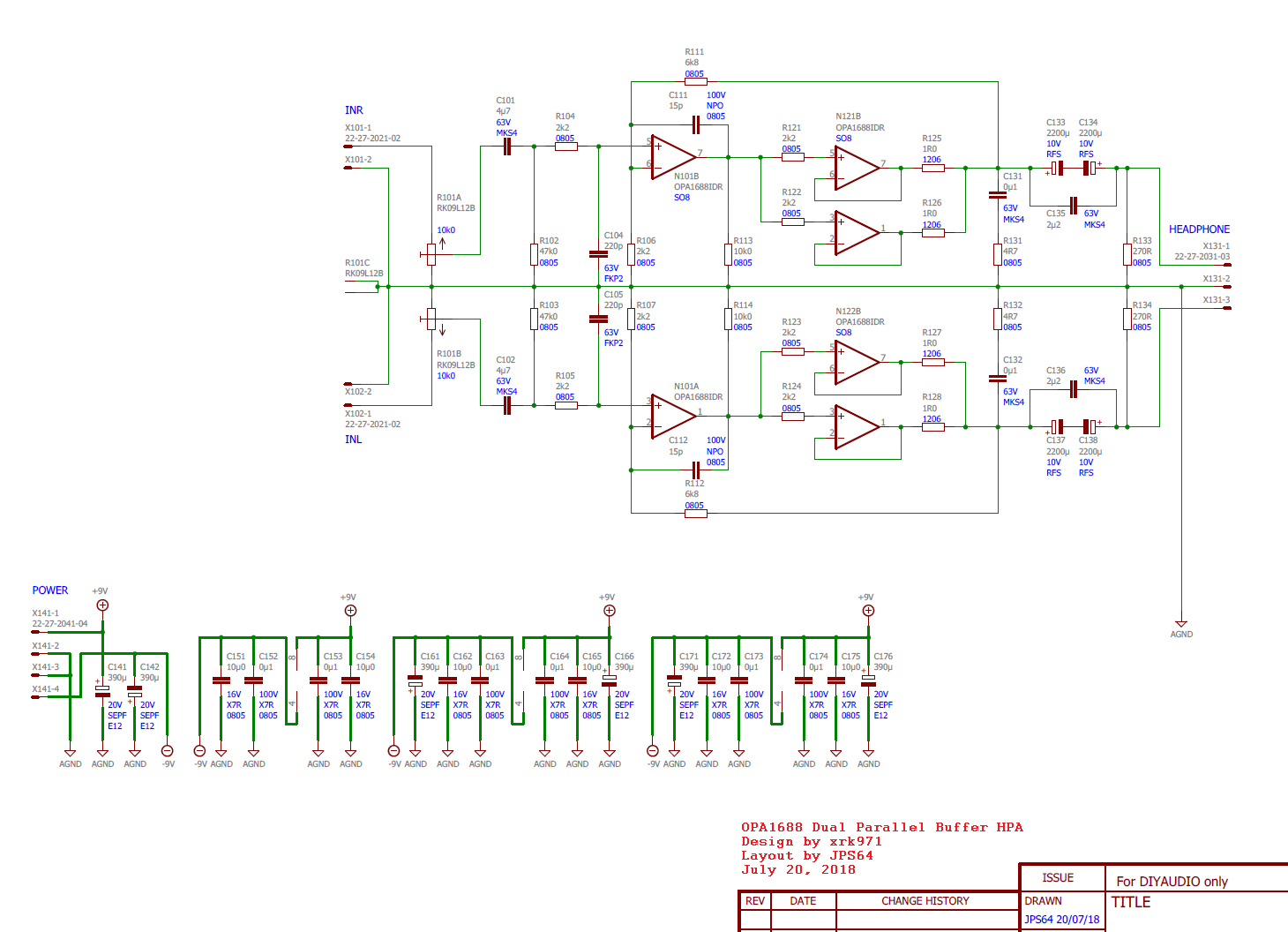
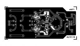
Files below: schematic, copper etch layer, and placement guides for top and bottom.
Schematic (note, for balanced opamp inputs (w/ pot at full volume) use R104 & R105 = 1.72k, and R111 & R112 should be high quality metal thin film, or carbon film, but not thick film):
Files below: schematic, copper etch layer, and placement guides for top and bottom.
Attachments

Last edited:
I can see that due to limitation of a single layer layout it is a bit hard to optimize position of the "output stage" supply rail lines. Since this is essentially a class B stage, those rails will be carrying rectified load current, which will induce even harmonics in signal tracks. For circuit like that it can be easily a limiting factor if it's driving a low impedance load. Using a twisted pair of a hook up wire to bring supply to those opamps can help to avoid this problem.
Very interesting chip.
Can you solder the 8-SOIC package directly to the bottom of a DIP-8 board? If so, then it makes it more DIY friendly.
I've avoided surface mount parts, but I have used a "power pack" package buffer. I made the board from scratch and used drop and mop soldering technique. Works great and I've been listening to the headphone amp for over 2 years.
I finally built the 2x Parallel Buffer OPA1688 HPA prototype with a hand etched board. I had some solder bridges with the skinny traces that went under a resistor that took a while to debug. I finally added a strip of Kapton over the under-passes to avoid problems. Will measure later, but listening to it now and sounds very good. Listened to a few tracks on headphones and the HE400-i's have no trouble being driven hard and loud. Using as a preamp on my Alpha BB speaker amp now.
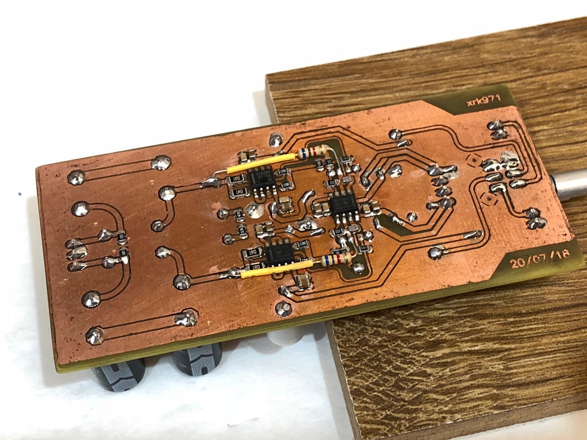
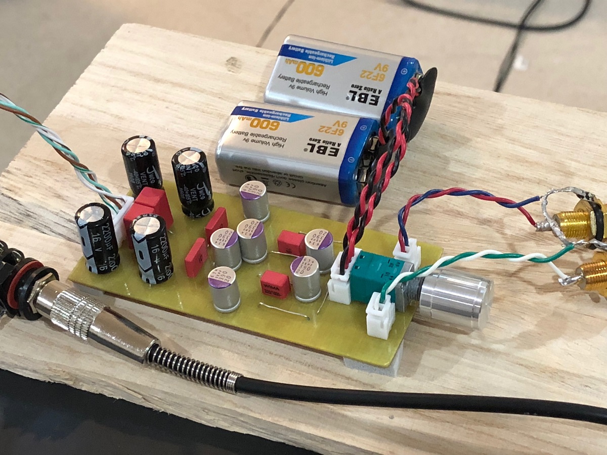
A big thanks to JPS64 for a super layout!
A big thanks to JPS64 for a super layout!
Attachments

Can you solder the 8-SOIC package directly to the bottom of a DIP-8 board? If so, then it makes it more DIY friendly.
You can find SOIC8 to DIP8 adapter boards easily.
For exakmple:
20pcs SOP8 SO8 SOIC8 TSSOP8 MSOP8 to DIP8 Adapter PCB DIY Conveter Board new N65 | eBay
I know that. But in the interest of going small, and adhering to general KISS principles, I would like to try my idea.
I did not know about these adapter boards when I built my current headphone amp, or else I would have used them. I did end up making some very handy buffer boards though, that had the "Power Pack" chip on them, a small heatsink, bypass capacitor array, output series resistor and protection diodes. These boards could be snatched out and used with a completely different circuit, which will probably happen.
I'm hoping to prototype a circuit using this chip with a "Perma-Proto" board. So thanks for the information!🙂
I guess I do not know what you mean by soldering an SOIC8 directly to the bottom of a DIP board? The pin spacings are all off, hence the need for the adapter board. What's a power pack chip? Maybe show us a photo of what you mean, and also photo of your proto board.
- Home
- Amplifiers
- Headphone Systems
- Cheap as Chips OPA1688 Low-THD Muscle Amp