Interesting observation, I hadn't even considered saturation of the optocoupler output transistors. Regarding the frequency response, isn't a low value a benefit in this application? Doesn't the bias value need to be held relatively constant whatever the signal?
Good question.
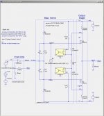
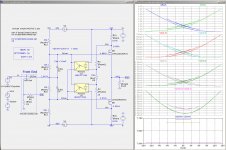
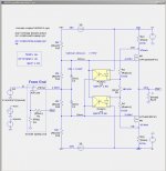
Here is a simulation where a "perfect" arbitrary current source replaces the series opto outputs. Because of SPICE limitations, a compute the LED currents from the voltage across 1m resistors connected to the rails.
The plots are:
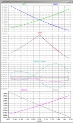
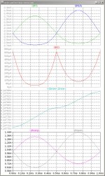
- waveforms vs. time of a 1kHz 1W signal into 4R from 0 secs to 3 secs.
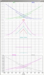
- 1 cycle of waveforms vs. time of a 1kHz 1W signal into 4R at 0 secs.
- 1 cycle of waveforms vs. time of a 1kHz 1W signal into 4R at 3 secs.
- 1 cycle of waveforms at vs.V(out) at 3 secs of a 1kHz signal in to 4R at 1W, 5W and 25W.
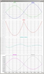
- 1 cycle of waveforms at vs.V(out) at 3 secs of a 1W signal in to 4R at 20Hz, 100Hz, 1kHz, and 10kHz.
Attachments
-
 series-perfect-bias-servo.asc.jpg163.1 KB · Views: 343
 -
 series-perfect-bias-servo-1W-4R-20Hz-100Hz-1kHz-10kHz-3secs-vs-Vout.jpg237.4 KB · Views: 112
 -
 series-perfect-bias-servo-1kHz-4R-1W-5W-25W-3secs-vs-Vout.jpg217.9 KB · Views: 291
 -
 series-perfect-bias-servo-1kHz-1W-4R-3secs-1cyc.jpg235.1 KB · Views: 305
 -
 series-perfect-bias-servo-1kHz-1W-4R-0secs-1cyc.jpg231 KB · Views: 317
 -
 series-perfect-bias-servo-1kHz-1W-4R-0secs-3secs.jpg79.4 KB · Views: 340
Isn’t the “big jump in bias current” at startup the result of C1 and C2 being charged by R2 and R3 respectively? I can see the caps are large values but I don’t know the resistor values so cannot determine the time constant.
Another observation is that this kind of bias circuit produces its “output” as a current whereas ideally the bias generator would provide a constant voltage, i.e. at low impedance. Not sure whether this is a problem though given the presence of the two capacitors.
Another observation is that this kind of bias circuit produces its “output” as a current whereas ideally the bias generator would provide a constant voltage, i.e. at low impedance. Not sure whether this is a problem though given the presence of the two capacitors.
No, SPICE computes the initial DC state, which includes the correct voltages across C1 and C2, before starting the transient waveform computation.
Thinking more about the opto transistor internal capacitances, the big one is the Miller capacitance from the collector to the base. The input impedance to the base of the transistor is another important parameter, but for a photo-transistor I have no idea how that input impedance is calculated.
No, SPICE computes the initial DC state, which includes the correct voltages across C1 and C2, before starting the transient waveform computation.
If that is the case, doesn't it suggest a problem with the steady state, I.e the output FETs are not conducting equally?
Regarding capacitance, do optocouplers even exhibit Miller capacitance?
If that is the case, doesn't it suggest a problem with the steady state, I.e the output FETs are not conducting equally?
Regarding capacitance, do optocouplers even exhibit Miller capacitance?
Yup, the photo-transistor has an emitter, base, and collector, but most optocouplers do not provide a connection to the base. See Photodiode - Wikipedia.
As soon as you see the results for the paralleled opto outputs, you will might cease to worry about the series optos.
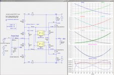
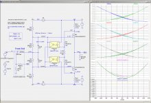
parallel optocoupler output bias circuits 1st try
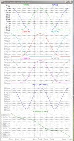
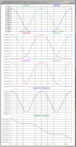
Switch just two wires in the series opto output circuit and you get the parallel opto output circuit. Here is a first attemp using resistor values similar to those in the series opto circuit. The first plots (2nd image) show the waveforms vs Vout for 20Hz, 100Hz, 1kHz, and 10kHz. Wow, this looks pretty good until you look at the last image showing the 1kHz waveforms at 1W, 5W, and 25W. The bias levels decrease significantly with wattage increase.
Switch just two wires in the series opto output circuit and you get the parallel opto output circuit. Here is a first attemp using resistor values similar to those in the series opto circuit. The first plots (2nd image) show the waveforms vs Vout for 20Hz, 100Hz, 1kHz, and 10kHz. Wow, this looks pretty good until you look at the last image showing the 1kHz waveforms at 1W, 5W, and 25W. The bias levels decrease significantly with wattage increase.
Attachments
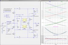
parallel optocoupler output bias circuits 2nd try
After increasing the resistor values significantly the sensitive to wattage is reduced, but not eliminated. The sensitivity to frequency (not shown) is not noticeably changed.
After increasing the resistor values significantly the sensitive to wattage is reduced, but not eliminated. The sensitivity to frequency (not shown) is not noticeably changed.
Attachments
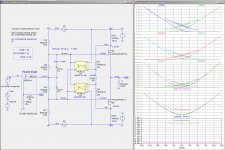
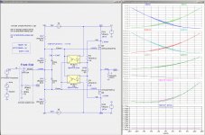
parallel optocoupler output bias circuits WOW!
After considerable experimentation I arrived at values the significantly reduces the sensitivity to wattage.
After considerable experimentation I arrived at values the significantly reduces the sensitivity to wattage.
Attachments
parallel optocoupler output bias circuits opto CTR mismatch
Here is something I did not expect. The parallel opto output circuit is rather insensitive to current-transfer-ratio (CTR) mismatch. Show are the waveforms optos whose CTRs differ by 3:1, but have the same CTR sum. If the sum is not the same, the Rcs resistor, which should really be a pot, must be adjusted.
You can see that the Ix(U1:C) and Ix(U2:C) transistor collector currents are now very different, and the Ix(U1:C)+Ix(U2:C) waveform is somewhat hifted to the left, but otherwise the waveforms are about the same as with matched CTRs. I did not expect this result.
Following posts will examine aspects of the circuit that have not been discussed: sensitivity to rail voltage and temperature.
Attachments

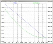
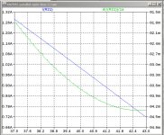
parallel optocoupler output bias circuits Rail voltage sensitivity
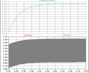
Here are some plots of bias current vs. rail voltage and its derivitive (dI/dV). The first plot corresponds to the "1st try" circuit values whose bias current vs. Watts was quite bad. The 2nd plot was for the "2nd try" circuit. You can see that the higher resistor values decrease dI/dV (magnitude).
Here are some plots of bias current vs. rail voltage and its derivitive (dI/dV). The first plot corresponds to the "1st try" circuit values whose bias current vs. Watts was quite bad. The 2nd plot was for the "2nd try" circuit. You can see that the higher resistor values decrease dI/dV (magnitude).
Attachments
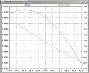
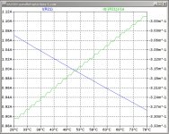
parallel optocoupler Rail voltage and temperature sensitivity - WOW!
And here the rail voltage sensitivity is nearly zero. And the final plot is the temperature sensitivity of the same circuit.
How believable are these simulations? The models used for the FETs and optocouplers are only approximations. The relationships between FET junction temperatures and optocoupler temperatures best guesses and are dependent on packaging, ventilation, and the phase of the moon. The values of Ropto1 and Rcs are the only adjustments available, but they should get close the the "optimal" results.
Attachments

Well, you have certainly given us plenty to think about!I’ve only had a quick look but I still have many questions. I’ll start with what I see as the key points and follow up on the other points later.
As an aside, this is a very similar circuit to the one I was experimenting with some time ago although I used a current source in place of Rcs (R5).
Increasing the values of Ropto1 decreases the sensitivity of the bias generator to changes in the current flowing through the FET output devices. As you have shown this is beneficial in reducing the sensitivity to changes as more signal related power is delivered to the load. However, I would expect larger values of Ropto1 to also negatively impact sensitivity to changes in the (bias) component of the output current that we are interested in keeping constant. Curiously your results of change in output current with varying supply voltage appear to contradict this so maybe I am wrong.
In any case, I anticipate the issue of reducing bias to return if the output power is increased further. Nelson addressed the same issue rather elegantly in the M2 with the addition of the LM385s. Perhaps a similar solution is required here?
Are ypu asking whether increasing the values of the Rcs and Ropto1 resistors results in lowering the negative feedback of the bias servo and if that results in poorer control of the bias?...
However, I would expect larger values of Ropto1 to also negatively impact sensitivity to changes in the (bias) component of the output current that we are interested in keeping constant. Curiously your results of change in output current with varying supply voltage appear to contradict this so maybe I am wrong.
In any case, I anticipate the issue of reducing bias to return if the output power is increased further. Nelson addressed the same issue rather elegantly in the M2 with the addition of the LM385s. Perhaps a similar solution is required here?
A possible way of measuring the amount of bias servo feedback is to compute the following:
gm(NFET) * d(VDrive+,Out)/d(I(RsenP))
gm(PFET) * d(V(Out,Drive-)/d(I(RsenN))
I am not sure how to do this properly, since the desired computation is the open-loop values. A better formulation is to compute the the values of d(V(Out,Drive-)/d(I(RsenN)) directly from the resistor values and the opto CTR, rather than measuring.gm(PFET) * d(V(Out,Drive-)/d(I(RsenN))
Last edited:
Yes, specifically Ropto1, although I wasn’t thinking of it in these terms. Actually it would be interesting to discover how effective the bias servo is in general given the low LED currents at which the optos are operating.
You are obviously more capable than I at mathematical analysis so I am not going to comment on your proposed approach to measuring the amount of negative feedback.
What about operation at higher powers? Are you not concerned that the bias will drop excessively?
You are obviously more capable than I at mathematical analysis so I am not going to comment on your proposed approach to measuring the amount of negative feedback.
What about operation at higher powers? Are you not concerned that the bias will drop excessively?
Do you mean amplifiers with higher maximum power or highe than 25W from the circuit I show? Here is an example of this circuit at 1kHz 100W into 2R. The first set of waveforms are at 0 secs where C1 and C2 are charged to the SPICE initial state giving 1.0A bias. The second set is at 2 secs, and the bias has been reduced to 0.8A, which is not really desirable. Note that the amplifier is running class-AB, with little overlap of simultaneous FET conduction.Yes, specifically Ropto1, although I wasn’t thinking of it in these terms. Actually it would be interesting to discover how effective the bias servo is in general given the low LED currents at which the optos are operating.
You are obviously more capable than I at mathematical analysis so I am not going to comment on your proposed approach to measuring the amount of negative feedback.
What about operation at higher powers? Are you not concerned that the bias will drop excessively?
Attachments
That is exactly what I meant. As the output stage moves increasingly into the class B region, the bias will reduce. Similarly for musical peaks. I believe we need something that forces a suitable minimum bias in this situation.
I dot really intend to run this amplifier class-AB. I would expect most people's use might only have an occasional transient into class-AB. The time constants of the C1-R12-R14 and C2-R13-R15 are about 26 seconds, so occasional class-AB transients should not be a problem.That is exactly what I meant. As the output stage moves increasingly into the class B region, the bias will reduce. Similarly for musical peaks. I believe we need something that forces a suitable minimum bias in this situation.
OK, I had mistakenly assumed that you were aiming for something similar to the XA25 which is good for 200W peak into 2 ohms.
Does this also mean that you are not interested in a frequency response down to DC (as per XA25)? Although C1 and C2 are large in your circuit, the output will still reduce at lower frequencies. Although I suspect that most of us will not wish to operate our amplifiers at DC, it is still an interesting challenge to solve.
Does this also mean that you are not interested in a frequency response down to DC (as per XA25)? Although C1 and C2 are large in your circuit, the output will still reduce at lower frequencies. Although I suspect that most of us will not wish to operate our amplifiers at DC, it is still an interesting challenge to solve.
- Home
- Amplifiers
- Pass Labs
- F4 Beast Builders