Hi Alchamist,
I was not trying to be unhelpful at all. You need to understand this stuff, not just know the steps. I realise my response was not what you wanted to hear, but I have taught technicians for years and am concerned you might end up with pretty large gaps in your understanding.
What I didn't do was tell you to go buy the text books and learn from that. I did try to impress upon you that there is a vast amount of background information to learn as well. So even though you have the answers, I am hoping you will take the time to learn the stuff behind this.
Just for my own curiosity, what instruments do you have now? That will help determine what information is useful to you and what isn't.
For clarification ...
2. input a stepped wave form and measure how long it takes the output to go from 10% to 90% of the final output level. Of course you must not clip the amplifier or the values will be invalid.
4. is normally done by measuring open circuit voltage compared to the loaded voltage. For power amplifiers this would be an 8 R load. Calculate the same way as posted above.
5. Measure your zero at some power level, normally just before clipping for power amps, then remove the signal and measure the noise level. SNR is the ratio between the two. For preamps or signal stages you would normally set your reference level at some signal level. I don't know what is industry standard these days. 0 dBu was a working standard, as was -10 dBu. Simulators normally do not calculate component noise levels and gain. So not possible in a normal simulator.
6. You measure peak voltage into an 8 R load (or 4 R if that is your spec) just before clipping. You can set with a triangle waveform as the peaks are easy to see. Take that level as your peak voltage and calculate watts from that point. Many designs can exceed 1% THD before getting close to the onset of clipping.
7. Measure a full signal in one channel, then measure the signal level in the other channel and that ratio gives you your cross-talk number.
8. It can be measured similarly to damping factor. Set a signal source to some level (1 volt is fine as long as you don't overdrive the input stage). Insert a resistance in series and measure across the input while increasing the series resistance. When the voltage reads 1/2 of the initial value, the series resistance = the input resistance.
You should be able to do everything except #7 in a simulator. All you need do is equate how you would measure these things in real life with the simulator. See? You have to understand the basics before accepting a test method in your simulator.
Simulators often give specifications that are not attained in real life unless you can input PCB characteristics and layout specific information. Too complicated to figure out all your variables. One thing is for sure though, your performance can not be any better than what the simulator spits out as long as the models are good. It also assumes that each and every value is exactly correct and does not vary over changing voltage and current levels (like real parts do). It also assumes that each transistor of the same part # is exactly the same. Not even close in real life, and that includes resistors, transistors and capacitors.
-Chris
Sorry folks, I placed an order for 4 channels' worth of TPA3255. I no longer need these boards.Unfortunately no longer need 4 boards, only 2.
454Casull - 2 boards
Rick G - 2 boards
Hajj - 4 boards
xrk971 - 2 boards
redarc12 - 2 boards
Rick G - 2 boards
Hajj - 4 boards
xrk971 - 2 boards
redarc12 - 2 boards
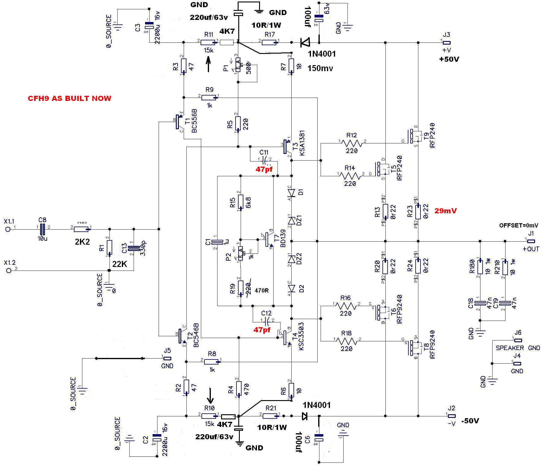
Error in layout CFH7 from Sonal
Hi X,
there is critical error in the CFH7 layout from SonaI (also the gerbers). All pins on the bias spreader transistor BD139 are shorted , see post #379 and the gerbers in the posts before. Possible to get the corrected version??
thanks
Günni
Hi X,
there is critical error in the CFH7 layout from SonaI (also the gerbers). All pins on the bias spreader transistor BD139 are shorted , see post #379 and the gerbers in the posts before. Possible to get the corrected version??
thanks
Günni
Hi X,
there is critical error in the CFH7 layout from SonaI (also the gerbers). All pins on the bias spreader transistor BD139 are shorted , see post #379 and the gerbers in the posts before. Possible to get the corrected version??
thanks
Günni
Yes Indeed, due to the central pad.
regards
Prasi
Yes Indeed, due to the central pad.
regards
Prasi
Exactly, and no one raised the finger. I had to modify my 2 CFHs and remove the shorts with a Dremel. Did really nobody build this version 😉?
BR
Gunni
PS: i informed Sonal months ago, but didn't get any response
@schillg11
Did the boards work other than having to dremel those traces? No other issues?
Wondering, because I'm looking for a winter project and might buy a few boards?
Did the boards work other than having to dremel those traces? No other issues?
Wondering, because I'm looking for a winter project and might buy a few boards?
after an interesting discussion about SCHADE in this topic
http://www.diyaudio.com/forums/pass-labs/314822-greedy-boy-defisit-papas-koans-14.html#post5280739
I made some simulations to change my CFH7 / VSSA, I still did not have time to put into practice due to the Christmas parties.
I decided to share if anyone else wants to try .... 2 new resistors were added between gate and drain and besides increasing the gate resistors I needed to change the VBE resistors.
merry christmas everybody
Thiago
Attachments
This formed the basis of my car amp in the 80's.
npn vas with 7 ma CCS and LF353 op amp servo to remove large caps
outstanding frequency response and detail.
I am placing a newer version into my SX-3700 vs Litschtark in sx780 detailed here
by Vzaichenko at High Fidelity Audio Equipment | Canada | VIRTUAL ZERO AUDIO
npn vas with 7 ma CCS and LF353 op amp servo to remove large caps
outstanding frequency response and detail.
I am placing a newer version into my SX-3700 vs Litschtark in sx780 detailed here
by Vzaichenko at High Fidelity Audio Equipment | Canada | VIRTUAL ZERO AUDIO
why the bias with R24 and R25?
bias T5 for 6.5v
for vies SCHADE, leaving the mosfet with the character tube triode
after an interesting discussion about SCHADE in this topic
http://www.diyaudio.com/forums/pass-labs/314822-greedy-boy-defisit-papas-koans-14.html#post5280739
I made some simulations to change my CFH7 / VSSA, I still did not have time to put into practice due to the Christmas parties.
I decided to share if anyone else wants to try .... 2 new resistors were added between gate and drain and besides increasing the gate resistors I needed to change the VBE resistors.
merry christmas everybody
Thiago
Does the sim show a difference to THD with Schade feedback?
I made some simulations to change my CFH7 / VSSA, I still did not have time to put into practice due to the Christmas parties.
I decided to share if anyone else wants to try .... 2 new resistors were added between gate and drain and besides increasing the gate resistors I needed to change the VBE resistors.
merry christmas everybody
Thiago
Nice to see VSSA still intrigues people. At so simple design every little change makes significant difference. Some resistor's values are stoned from VSSA's era on and it looks not much's gonna change either. Adding Rgd-s decreases OLGNF which for stability sake really is unnecessary, VSSA HF square response is almost perfect and that alone tells a lot. Dumping beneficial gain will only result into higher THD, which we obviously don't want at already mild THD amp. What I would work on is to make VAS more 'isolated' from output's stage influences. There are some simple measures to achieve this without increasing overall complexity. Using ultra high quality parts also helps.

Does the sim show a difference to THD with Schade feedback?
a little, I do not know if it would be an audible change, maybe there is something in Triode-Schade-Mode that goes beyond the harmonious profile.
Nice to see VSSA still intrigues people. At so simple design every little change makes significant difference. Some resistor's values are stoned from VSSA's era on and it looks not much's gonna change either. Adding Rgd-s decreases OLGNF which for stability sake really is unnecessary, VSSA HF square response is almost perfect and that alone tells a lot. Dumping beneficial gain will only result into higher THD, which we obviously don't want at already mild THD amp. What I would work on is to make VAS more 'isolated' from output's stage influences. There are some simple measures to achieve this without increasing overall complexity. Using ultra high quality parts also helps.
Thanks for the tips and comments lazy cats. I'm from Nelson Pass School and I'm a fan of some harmonized controlled profile. I did not have a good experience with the CFA, I mounted PeeCeeBee, CFH7 and A33 Apex and all 3 found it difficult and lifeless, very accurate, but it was not what I was looking for. all 3 very stable and an incredible bandwidth, plus I still prefer Quasi from Ranchu, ACA with 24v from Nelson Pass and AX11 Apex that sounds incredible to me with a lot of footprint and a sweet sound. I do not want to do a discussion here, but do I want THD too low? Maybe it's my ears, or my speakers. Thank you for VSSA that you introduced the community, without a doubt, an excellent amplifier.
Thiago
Thiago,
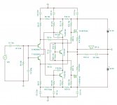
Perhaps you might like the harmonic profile of the Aksa Lender Preamp. Then use that to drive any output stage topology. Even the CFH7 juat strip off everything except output and vbe multiplier and connect Aksa Lender. It is low distortion and nice harmonic profile you like.
AKSA's Lender Preamp with 40Vpp Output
AKSA's Lender Preamp with 40Vpp Ouput GB
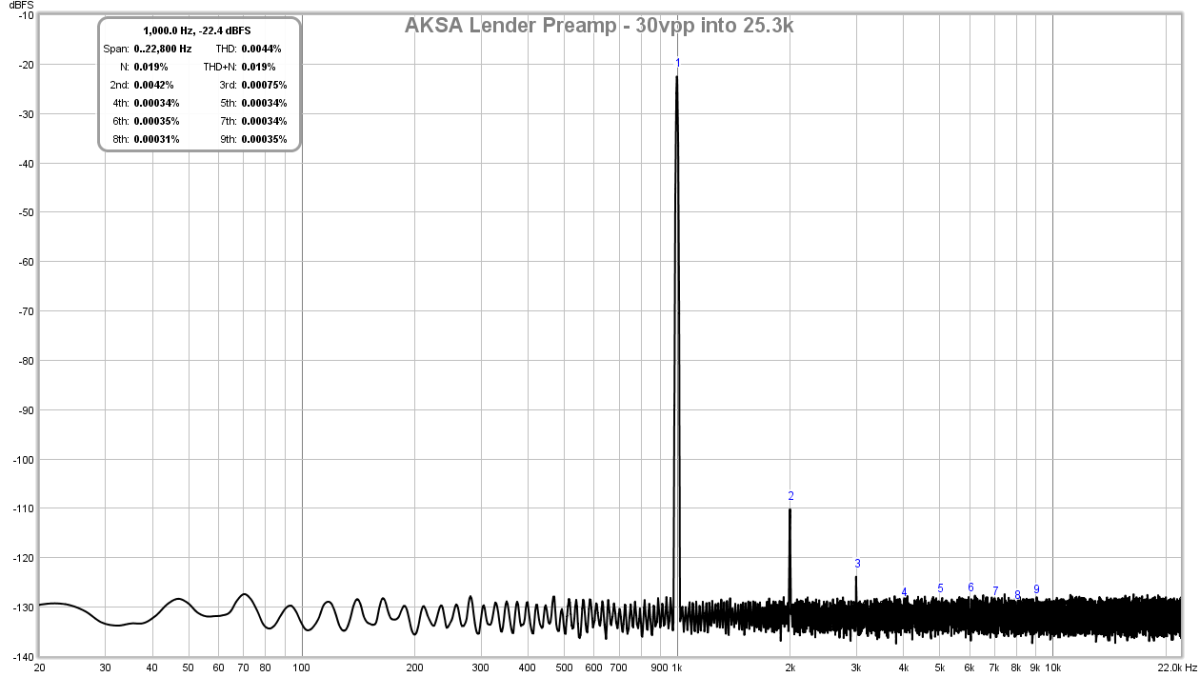
Here is the preamp driving 30vpp into 25kohm load (although still very similar even at 7kohm load):
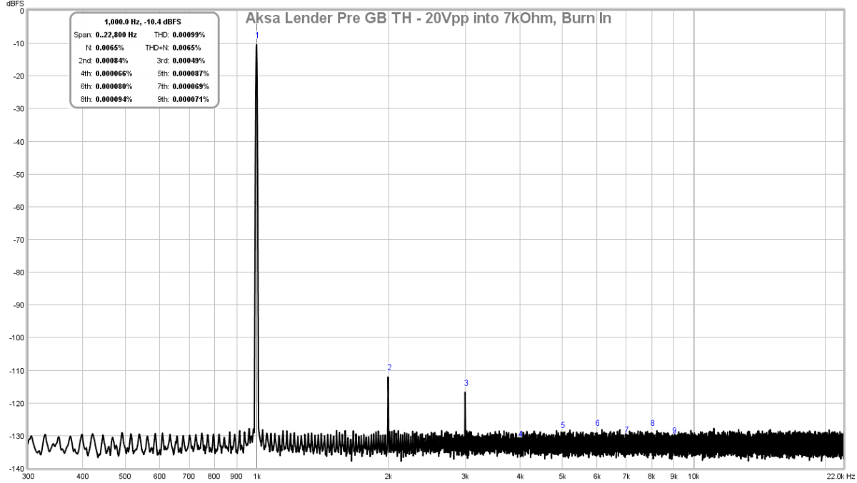
Here is 20vpp into 7kohm load:
Perhaps you might like the harmonic profile of the Aksa Lender Preamp. Then use that to drive any output stage topology. Even the CFH7 juat strip off everything except output and vbe multiplier and connect Aksa Lender. It is low distortion and nice harmonic profile you like.
AKSA's Lender Preamp with 40Vpp Output
AKSA's Lender Preamp with 40Vpp Ouput GB
Here is the preamp driving 30vpp into 25kohm load (although still very similar even at 7kohm load):
Here is 20vpp into 7kohm load:
Last edited:
Hay diyers,
I just finished 4 Thiagomogi's boards from post #962,and again I have problem with no bias on all 4 boards. In past I was have a problem with one board ,and I was changing bias trimer from 1 kohm to 5 kohm and that do the trick. Now all 4 boards have 5 kohm bias trimer but I can not get any current on all 4 board. I double checked all values of elements and I can not find what is wrong.
Here are some voltage on BD139 transistors:
Board 1
Base - GND = 1.88V
Collector - GND =2.78V
Emitter - GND = 1.22V
Board 2
Base - GND = - 1.9V
Collector - GND = 1.13V
Emitter - GND = -3.0V
Board 3
Base - GND = 1.58V
Collector - GND = 2.73V
Emitter - GND = 1.58V
Board4
Base - GND = 2.7V
Collector - GND = 2.7V
Emitter - GND = 2.7V
All voltage are referred to GND ,no input signal,no output load,power supply is +-43V.
Any suggestion how to solve that problems?
Regards
zoky2
Hay diyers,
I just finished 4 Thiagomogi's boards from post #962,and again I have problem with no bias on all 4 boards. In past I was have a problem with one board ,and I was changing bias trimer from 1 kohm to 5 kohm and that do the trick. Now all 4 boards have 5 kohm bias trimer but I can not get any current on all 4 board. I double checked all values of elements and I can not find what is wrong.
Here are some voltage on BD139 transistors:
Board 1
Base - GND = 1.88V
Collector - GND =2.78V
Emitter - GND = 1.22V
Board 2
Base - GND = - 1.9V
Collector - GND = 1.13V
Emitter - GND = -3.0V
Board 3
Base - GND = 1.58V
Collector - GND = 2.73V
Emitter - GND = 1.58V
Board4
Base - GND = 2.7V
Collector - GND = 2.7V
Emitter - GND = 2.7V
All voltage are referred to GND ,no input signal,no output load,power supply is +-43V.
Any suggestion how to solve that problems?
Regards
zoky2
Replace 6k8 with 12k in bias circuit.
apexaudio,
I replaced 6k8 resistor with 12k and still no change . Something other must be wrong🙁🙁
Regards
zoky2
I replaced 6k8 resistor with 12k and still no change . Something other must be wrong🙁🙁
Regards
zoky2
It’s been a while since this amp has received any attention. Thimios debugged it and the good schematic is here:
Is there any interest in a new layout with state of art layout methods? Although the layout by Thiago is also excellent looking.

Is there any interest in a new layout with state of art layout methods? Although the layout by Thiago is also excellent looking.
Last edited:
apexaudio,
I replaced 6k8 resistor with 12k and still no change . Something other must be wrong🙁🙁
Regards
zoky2
Did you ever resolve the lack of bias issue?
- Home
- Amplifiers
- Solid State
- CFH7 Amp