Member
Joined 2009
Paid Member
I just realized that R10 (series feedback res) is 1/2W instead of 1W as per BoM. Should I change this or I'm fine with 1/2W?
I just need to clean the underneath of the PCB, then I can fire up this amplifier for testing.
Thanks
Do
I wouldn't worry at this point. I don't think it will be an issue.
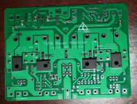
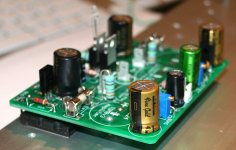
So here's some new pictures
I'm a bit confused by C3's orientation now... Please let me know if ok. I have the latest PCB, B rev and latest schematics shows negative to gnd, which I did but then I read it was the opposite which I believe also it should be..? Am I right? If yes, then C3 needs to be swapped around.


I realized that C17 and C19 are not mandatory and I will most likely remove them.
Ciao!
Do
I'm a bit confused by C3's orientation now... Please let me know if ok. I have the latest PCB, B rev and latest schematics shows negative to gnd, which I did but then I read it was the opposite which I believe also it should be..? Am I right? If yes, then C3 needs to be swapped around.
I realized that C17 and C19 are not mandatory and I will most likely remove them.
Ciao!
Do
Hi Bigun,
For the speaker output, would a simple output zobel (10R 5W resistor in series with 47nF cap placed accross output + and gnd) suffice or should I make an inductor?
If it's better to use an inductor, I have some 14awg (1.65mm) enamel wire. If I use a AA battery, how many turns would you suggest?
Thanks
Do
The amplifier output Zobel is an R+C from Output back to decoupling capacitors.
It forms a High Frequency load
The Thiele Network is a combination of the output Zobel and a load isolating damped inductor.
Many will build with only an output Zobel. I do not recommend this.
Some build with the Thiele Network. Download Dr Cherry's papers and read thoroughly. They are on this Forum, but will take a bit of searching.
Following on from Dr Cherry's papers I came to realise that the two versions proposed by Neville Thiele are not exclusive to each other.
I now use both arrangements in a Pi filtering Network.
C+R across the output to decoupling capacitors.
L||R in the internal speaker feed cable.
C+R across the amplifiers output terminals.
Cherry, Leach and Cordell refer to this last C+R and none of them have anything adverse to say about adding it to the build.
Member
Joined 2009
Paid Member
I am still at work - let me look at this in more detail once I am home (later this evening as I am working late today). I'm afraid all the power devices are incorrectly installed - do not power it up yet!
I am still at work - let me look at this in more detail once I am home (later this evening as I am working late today). I'm afraid all the power devices are incorrectly installed - do not power it up yet!
Oh... they go under the PCB? Not a problem if it's how they're installed. Can be fixed pretty quickly. Thought the holes were just for holding the board on the heatsink...
I'll wait for your input.
Thanks
Do
Member
Joined 2009
Paid Member
Yes, the power devices go under the board !
I guess they don't have to, but if you mount them out to the side like you did, they need to be the other way up, shiny side facing upwards or the pins are reversed.
To mount them underneath you need spacers between the power device and the underside of the pcb. There are photos and descriptions in the thread somewhere. Here (attached) is a photo to show you how I made spacers. I used some extra TO-126 packaged transistors, BD139 probably. The advantage is that they are of uniform thickness, have holes of just the right size. I cut the leads down so that only the centre lead is left just a short bit, then I use it to solder the spacer-transistor to the board. It's not a great way to make an amplifier and I don't do it exactly like this on other designs but it does work. Look at the photo, it shows the spacer-transistors in place. You don't need to solder them, you can stick them on with some glue instead - probably much easier. It's best to bolt the spacer-transistors to the board when you solder/glue them so that the holes are properly aligned with the holes in the pcb.
Attachments
Member
Joined 2009
Paid Member
Attached here is another photo that shows how the power devices fold underneath the pcb. To ensure that the power devices are installed properly I recommend the following procedure, after you first install the spacers.
You bend the leads of the power devices the right way and install them into the pcb without soldering. You'll have to clean up the solder from the holes first. Then you bolt the assembly to the heatsink, a bolt through all of the power devices. This forces the power devices to be flat against the spacers, and flat to the heatsink. Then you solder the leads to the pcb. When you remove the assembly from the heatsink the devices will be attached to the pcb all properly aligned and parallel.
You bend the leads of the power devices the right way and install them into the pcb without soldering. You'll have to clean up the solder from the holes first. Then you bolt the assembly to the heatsink, a bolt through all of the power devices. This forces the power devices to be flat against the spacers, and flat to the heatsink. Then you solder the leads to the pcb. When you remove the assembly from the heatsink the devices will be attached to the pcb all properly aligned and parallel.
Attachments
Member
Joined 2009
Paid Member
Here's another image (attached). It shows the power devices (just two of them) installed on the underside, with the spacer transistors between them and the pcb. This is a photo of the build by Christian (Ranchu32) who was the first person to assemble the amp on the original board (he had nice blue coloured boards!). The bolts he installed for this photo are temporary - however, I recommend bolting the assembly to the heatsink when soldering the power devices instead.
Attachments
Last edited:
Yeah, pretty easy to fix on my side. Don't know why I didn't think they were going under the PCB... I thought the holes were in a weird place but knowing they go under, it all make sense! LOL
Thanks
Do
Thanks
Do
Member
Joined 2009
Paid Member
I hope it isn't too much hassle. I find getting power device out of a pcb to be painful - usually have to cut the leads off at the pcb level, desolder the metal pins from the pcb holes one at a time. This results in the leads being too short to re-use the power devices (you can guess how I know this!). So be prepared for some 'loss' of parts - all part of the learning process I'm afraid ! But this design has at least the advantage that it achieves high power without the need for matched pairs of output devices so if you blow them up it's cheaper to replace !
zobel - it's already on the board, R19 and C12 I believe. I like to keep the zobel close to the output devices, especially on such a 'fast' amplifier as this.
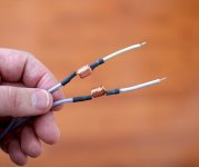
output inductor - yes, good idea to use one. In this design I kept it off-board. I placed it in the speaker wire between the pcb and the speaker binding post inside the chassis. See photo (attached).
zobel - it's already on the board, R19 and C12 I believe. I like to keep the zobel close to the output devices, especially on such a 'fast' amplifier as this.
output inductor - yes, good idea to use one. In this design I kept it off-board. I placed it in the speaker wire between the pcb and the speaker binding post inside the chassis. See photo (attached).
Attachments
Last edited:
No worries for desoldering, I've been doing this since I was 10 or so... over 30 years of experience on the iron. I'll fix it and post new picture of my corrected mistake... yep! My bad!
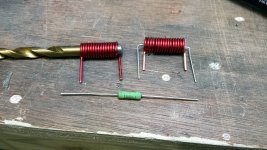
For the output inductor, how many turns would you put on it approximately if wounded over a double A battery? Or you can give me approx value and I will find an online Calc to find diameter, wire size and number of loops.
Thanks a million!
Do
For the output inductor, how many turns would you put on it approximately if wounded over a double A battery? Or you can give me approx value and I will find an online Calc to find diameter, wire size and number of loops.
Thanks a million!
Do
Member
Joined 2009
Paid Member
I dont think it needs to be exact, something like 15 to 20 turns around a pencil should do it. Its usually recommended to solder a 10R to 15R power resistor in parallel with the inductor. See attachee image I found on the internet. Youre looking for something in the range 1 to 2uH.
Attachments
Last edited:
I dont think it needs to be exact, something like 15 to 20 turns around a pencil should do it. Its usually recommended to solder a 10R to 15R power resistor in parallel with the inductor. See attachee image I found on the internet. Youre looking for something in the range 1 to 2uH.
Perfecto! Will add this for safety to the build
Thanks
Do
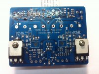
Here's the corrected transistor setup. No BJTs or Mosfets were harmed during the process! Hehe
I saved all devices and tested them, also checked all resistors around to ensure none got damaged. screws and nuts are just there to align everything when soldering.


Thanks for letting me know Bigun! Good thing I posted some pictures!
Do
I saved all devices and tested them, also checked all resistors around to ensure none got damaged. screws and nuts are just there to align everything when soldering.
Thanks for letting me know Bigun! Good thing I posted some pictures!
Do
What about C3, do I have the correct orientation? I believe I have to reverse it, after reading a post, seem to suggest it was wrong on the schematic.
Thanks
Do
Thanks
Do
Is it possible to modify this amp into a headphone amp? e.g. use a diamond buffer with smaller transistors for the power stage instead, and in this way one can avoid those small oscillations in the square wave response.
Member
Joined 2009
Paid Member
For a headphone amp why not use a Class A design, no feedback means no worry about your square waves! - there are a lot of designs on the 'net already and many on this forum that you might like. Some of them use DB output stages.
Be careful with square wave tests, you are looking for high frequency effects and cables, connectors, reflections etc. become an issue. My tests tend to be a bit rough-and-ready. So long as any wiggles are relatively small and well damped, the zobel is cold, the dc-bias is stable, and the sound is good - I'm satisfied.
Be careful with square wave tests, you are looking for high frequency effects and cables, connectors, reflections etc. become an issue. My tests tend to be a bit rough-and-ready. So long as any wiggles are relatively small and well damped, the zobel is cold, the dc-bias is stable, and the sound is good - I'm satisfied.
Last edited:
For a headphone amp why not use a Class A design, no feedback means no worry about your square waves! - there are a lot of designs on the 'net already and many on this forum that you might like. Some of them use DB output stages.
Hi Bigun,
thanks for your reply. I just read some post within this thread, and thought perhaps the small oscillations on the rising edge are caused by the hybrid output Stage with local feedback? if so, I can try to replace the output stage with simpler topologies and test it in my headphone system. The overshoots don't concern me, will have to adjust the compensation anyway for a low gain version like headphone amp.
The Singleton Input Stage looks really interesting to me.
Z
- Home
- Amplifiers
- Solid State
- TGM8 - my best amplifier, incredible bass, clear highs, no fatigue (inspired by Rod Elliot P3a)