Hi! picman.
this may be your answer .
I recently designed and made proto type multi channel DAC board for OPPO 203.
My intention of designing this DAC board is to take out the best sound for multi channel audio source (Multi channel SACD /DSD file) as well as surround movie sound.
Features.
1. premium Sabre ESS9038PRO DAC chip
2. best possible op amps: OPA2134 and OPA134 for each channel
3. ground isolation between OPPO main board and DAC section with opto coupler
4. separated clock (TCXO Japan NZ2520SD-80MHz : 20 ppm).
5. intensive use of local linear power supply (total 10 )
- separate analog and digital section of DAC chip .
- separate left and right section of DAC chip .
- dedicated power for 80 MHz clock
In OPPO DAC design, the biggest concern is digital 5V supply.
it derives from +15v DC supply.
So the 5V regulator dissipate 10V in vain and always runs very hot.
after 1 year use, all OPPO player's 5V regulator's back glue paint become dark.
OPPO 101 became with good solution.
OPPO 101's DAC board get digital power 5V from main board.
But OPPO 203 turns back to same as OPPO 93/103.
If you want to enhance the existing OPPO 203's multi channel DAC sound, change coupling capacitors.
Notice CE1,2,8,11,19,20,25,26.
existing coupling capacitors are ELNA 100uF 16V electrolytic capactior.
exchange it with 10UF OXCON ( 100uF for front l,R and sub woofer ) with 1uF Wima film capacitor ( 1uF/63v).
It will bring you remarkable sound improvement.
it is simple DIY work , but reward is big.
OPPO 203's AK 4458 DAC chip is inexpensive ( around 5 $ if I remember correctly ) .
so it is widely used in smartphone design . but it gives very natural sound.
Last edited:
this is the images for upgrading OPPO 203 DAC board.
if you want to listen 2 channel stereo music mostly, upgrade only Front L,R channel.


if you want to listen 2 channel stereo music mostly, upgrade only Front L,R channel.
Last edited:
This might help.
Feel free to ask any question.


Daughter board for anlaog section
출처: Jae H. Lee Blog :: high end 7.1 channel DAC for OPPO 203 [Jae H. Lee Blog]

Feel free to ask any question.
Daughter board for anlaog section
출처: Jae H. Lee Blog :: high end 7.1 channel DAC for OPPO 203 [Jae H. Lee Blog]
Hi, Jae Hung Lee,
Nice project......🙂
Are you actually going to sell this multi channel DAC board for OPPO 203, or is is just a nice research project for you.
And if you are going to take this in production and sell it, can you give a indication of the price.
Regards,
Jack
Nice project......🙂
Are you actually going to sell this multi channel DAC board for OPPO 203, or is is just a nice research project for you.
And if you are going to take this in production and sell it, can you give a indication of the price.
Regards,
Jack
Hi! picman.
this may be your answer .
I recently designed and made proto type multi channel DAC board for OPPO 203.
My intention of designing this DAC board is to take out the best sound for multi channel audio source (Multi channel SACD /DSD file) as well as surround movie sound.
Features.
1. premium Sabre ESS9038PRO DAC chip
2. best possible op amps: OPA2134 and OPA134 for each channel
3. ground isolation between OPPO main board and DAC section with opto coupler
4. separated clock (TCXO Japan NZ2520SD-80MHz : 20 ppm).
5. intensive use of local linear power supply (total 10 )
- separate analog and digital section of DAC chip .
- separate left and right section of DAC chip .
- dedicated power for 80 MHz clock
Hi! mdanielse.
I don't have any plan for making more multi channel DAC board right now.
it is answer to my friend's wish to have nice multi channel DAC board using ESS9038 pro chip.
He wanted this for his huge collection of SACD, especially multi channel SACD .
I have already made 2 channel ESS9038pro chip DAC board for OPPO UDP 203 as shown below .
so it is not that difficult to extend to multi channel board.
Due to space limitation, daughter board for 4 channel analog outputs , is needed.
6V AC winding is needed for reliable operation for digital section power supply .
it feeds clean 5V DC .
I don't have any plan for making more multi channel DAC board right now.
it is answer to my friend's wish to have nice multi channel DAC board using ESS9038 pro chip.
He wanted this for his huge collection of SACD, especially multi channel SACD .
I have already made 2 channel ESS9038pro chip DAC board for OPPO UDP 203 as shown below .
An externally hosted image should be here but it was not working when we last tested it.
so it is not that difficult to extend to multi channel board.
Due to space limitation, daughter board for 4 channel analog outputs , is needed.
6V AC winding is needed for reliable operation for digital section power supply .
it feeds clean 5V DC .
Last edited:


I have extra 2 channel stereo DAC board( blank ) for OPPO 203 as well as oppo 103(D).
if you pay shipping cost , I can send you along with schematics and part list ( BOM file) .
It is blank one( blue , gold plated PCB) .
You can do your own experiments .
This PCB has special provision for I2S data transmission to out of OPPO 103/203 .
please send PM.

if you pay shipping cost , I can send you along with schematics and part list ( BOM file) .
It is blank one( blue , gold plated PCB) .
You can do your own experiments .
This PCB has special provision for I2S data transmission to out of OPPO 103/203 .
please send PM.
Last edited:
Hi Jae Hong,
PM sent.
Thanks for sharing your work.
Could you post the schematics in higher resolution? Its not visible clearly as posted.
I had a few questions on your multichannel design
1. What analog IV design did you choose. I heard that due to higher current drive from the ES9038, IV design is a challenge
2. Did you measure THD, Noise performance of your multi-channel design?
3. What are you using to control the software registers in ES9038?
4. What scheme have you used for volume control?
5. How many layers does the PCBs use
6. Was a balanced output stage considered?
thanks
Last edited:
looks like the pictures are available in higher resolution on your website. So you dont have to repost here.
thanks
thanks
Hi.
Those who want to have schematics in detailed PDF form.
Send me PM with e mail address.
I don't want to open futher more informations and discussion in here .
Main reason is that I have to spend too much time in writing in Eglish.
Those who want to have schematics in detailed PDF form.
Send me PM with e mail address.
I don't want to open futher more informations and discussion in here .
Main reason is that I have to spend too much time in writing in Eglish.
Hi Jae (and Hi to Coris too)
Nice work. But I have a question or two to ask.
In the new Stereo and Multi-Channel boards, you seem to be using 80MHz rather 100MHz. Is there no particular reason or do you prefer 80MHz?
Also, on the picture below:
I see that you are re-clocking 27MHz. That goes into the main MediaTek chip. There is also a 25MHz clock on the smaller chip partner as well.
I have a sneaky suspicion, one that I have voiced privately with Coris, that the most important clock is the clock that initiates the processing of the data, that reads the data. If there is a RAM buffer, then the data is largely dormant, but then it is the first clock after the RAM memory that is the 'primary' clock. But the data has to be stored for a period of time and then read - that is the clock and the effect of that clock cannot be entirely undone by a later clock.
There is no particular reason in a technical sense, that I can completely explain the above. But then again, I was the first to point out to Coris that in the Oppo 95 (and later 105) that he needed to do more than just clock the ESS Sabre DAC, but the motherboard clock as well. Coris was initially reluctant to do that - but my assurances led him to be the second and he then realised it was true. We don't have a complete explanation for that either (would be glad if you could).
So what I am proposing is not entirely new. It was thought the DAC was the only important one. But everybody now knows that is not true. Now I am taking the a step further and asking the question.
The new hypothesis described above, is that the first clock is actually more important than the subsequent DAC clock. I have worked on that assumption for a while now and it seems to stack up with the results that we have been getting. I wonder which clock does that in the 203, is it the 25MHz and not the 27MHz. One of them has to be the 'important' one.
Thoughts are welcome.
Cheers, Joe
.
Nice work. But I have a question or two to ask.
In the new Stereo and Multi-Channel boards, you seem to be using 80MHz rather 100MHz. Is there no particular reason or do you prefer 80MHz?
Also, on the picture below:

I see that you are re-clocking 27MHz. That goes into the main MediaTek chip. There is also a 25MHz clock on the smaller chip partner as well.
I have a sneaky suspicion, one that I have voiced privately with Coris, that the most important clock is the clock that initiates the processing of the data, that reads the data. If there is a RAM buffer, then the data is largely dormant, but then it is the first clock after the RAM memory that is the 'primary' clock. But the data has to be stored for a period of time and then read - that is the clock and the effect of that clock cannot be entirely undone by a later clock.
There is no particular reason in a technical sense, that I can completely explain the above. But then again, I was the first to point out to Coris that in the Oppo 95 (and later 105) that he needed to do more than just clock the ESS Sabre DAC, but the motherboard clock as well. Coris was initially reluctant to do that - but my assurances led him to be the second and he then realised it was true. We don't have a complete explanation for that either (would be glad if you could).
So what I am proposing is not entirely new. It was thought the DAC was the only important one. But everybody now knows that is not true. Now I am taking the a step further and asking the question.
The new hypothesis described above, is that the first clock is actually more important than the subsequent DAC clock. I have worked on that assumption for a while now and it seems to stack up with the results that we have been getting. I wonder which clock does that in the 203, is it the 25MHz and not the 27MHz. One of them has to be the 'important' one.
Thoughts are welcome.
Cheers, Joe
.
Last edited:
Hi! Mr. Joe Rasmussen .
In other DAC forum, I found that NDK NZ2520SD is Ultralow phase noise oscillators from Japan and better than well known CCHD-957 in terms of phase noise in audible frequency .
NDK NZ2520SD is developed for manily digital audio application .
But only 80 Mhz is available.
My DAC PCB design has provision for installing CCHD-957 .
Again sorry for my poor English.
Read this for more info.
USB AUDIO | H i F i D U I N O
I have buaght in here.
NDK NZ2520SD 3.3V 80Mhz 49.152Mhz 45.1584Mhz 24.576Mhz 22.5792Mhz 12Mhz Ultra low phase noise oscillator - DIYINHK
In other DAC forum, I found that NDK NZ2520SD is Ultralow phase noise oscillators from Japan and better than well known CCHD-957 in terms of phase noise in audible frequency .
NDK NZ2520SD is developed for manily digital audio application .
But only 80 Mhz is available.
My DAC PCB design has provision for installing CCHD-957 .
Again sorry for my poor English.
Read this for more info.
USB AUDIO | H i F i D U I N O
An externally hosted image should be here but it was not working when we last tested it.
I have buaght in here.
NDK NZ2520SD 3.3V 80Mhz 49.152Mhz 45.1584Mhz 24.576Mhz 22.5792Mhz 12Mhz Ultra low phase noise oscillator - DIYINHK
Last edited:
sorry in my error in previous reply
not the image . but the link of NDK products .
here is correct one.
日本電波工業株式会社
not the image . but the link of NDK products .
here is correct one.
日本電波工業株式会社
Have you rechecked their claim of low noise by DIYINHK? It seems there is inconsistancy between their graphs and NDK's.Hi! Mr. Joe Rasmussen .
In other DAC forum, I found that NDK NZ2520SD is Ultralow phase noise oscillators from Japan and better than well known CCHD-957 in terms of phase noise in audible frequency .
NDK NZ2520SD is developed for manily digital audio application .
But only 80 Mhz is available.
My DAC PCB design has provision for installing CCHD-957 .
Again sorry for my poor English.
Read this for more info.
USB AUDIO | H i F i D U I N O
An externally hosted image should be here but it was not working when we last tested it.
I have buaght in here.
NDK NZ2520SD 3.3V 80Mhz 49.152Mhz 45.1584Mhz 24.576Mhz 22.5792Mhz 12Mhz Ultra low phase noise oscillator - DIYINHK

In the NDK graph, the blue dotted line indicates NZ2520SD, which is shown with red line in the DIYINHK's. Though the frequencies is different(49 vs 22), but it won't lead to such big difference in phase noise.
Did I miss something?
Did I miss something?
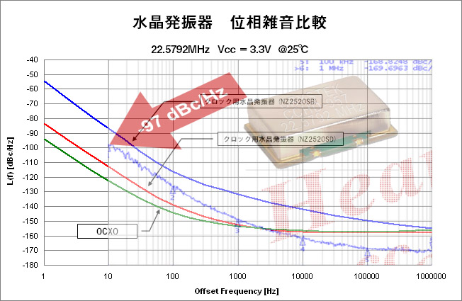
Hi. Arteck.
Below graph. Red line has less phase noise than Cryteck tcxo in the region of 10 ~ 4000hz which is most
Important audible range.
Below graph. Red line has less phase noise than Cryteck tcxo in the region of 10 ~ 4000hz which is most
Important audible range.
Hi. Arteck.
Below graph. Red line has less phase noise than Cryteck tcxo in the region of 10 ~ 10000hz which is most
Important audible range.
Yes. But I'm afraid the red line is not a real measure result. It's far too low than the NDK graph.
The new version of my Clock board (battery powered). Mainly the same approach as before (SAW oscillator for 27Mhz, and high quality TXCO for 25Mhz), and now using a smaller battery. The board is designed to fit for use on all Oppo models.
Attachments

- Home
- Source & Line
- Digital Source
- Oppo new UDP series players - 203/205 - Discussions, upgrades, modifications