I also suggest to check again resistances and solder joints of R16, R18, R20 if you have desoldered Q14.
Agreed. Please check all the resistors around Q14.
Have you replace Q14 before? Somehow I thought you might have done that once
already, but perhaps I was confused. 🙂
Hope you get this resolved soon.
Dennis
Have you replace Q14 before? Somehow I thought you might have done that once
already, but perhaps I was confused. 🙂
Hope you get this resolved soon.
Dennis
Yahooo replaced Q14 that did it....bad TL431 what pain! Thanks for your help...
Next hurdle since I did not buy my Vfet's from NP (I bought them from circuitdiy way back when NP first published the article) any way mine do not have the Vgs rating so whats the best starting voltage for P1, P2 ??
Next hurdle since I did not buy my Vfet's from NP (I bought them from circuitdiy way back when NP first published the article) any way mine do not have the Vgs rating so whats the best starting voltage for P1, P2 ??
Forgot: The Supplementary kit costs $155
hi mark,
could you please post the latest version of BOM for the supplemental kit?
many thanks and regards
Thanks
That's great!
I am very pleased at the success of you!
Clearly seen, for me one of my brain cells there is no need for.
So one of them, the treatment should be continued using red wine.
I'll get it somehow. 🙂
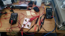
I strongly suggest to power on with VFETs, you must use a light bulb tester.
If you have variac as well, use both.
For first startup, I have set up variac to get about half of DC power voltage.
In my case, measured voltage across R32 started to going higher below cc. 13-14VDC power supply voltages, indicates increasing current on closing VFETs.
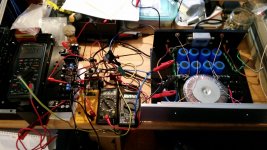
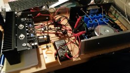
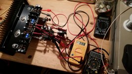
I've had an interesting weekend. Measuring Vgs of the VFETs sourced from Acronman, biasing up the frontend, installing the VFETs and biasing up the output stage.
So far everything looks good, I got the frontend offset down to about 50mV, and with the VFETs installed the total output offset down to single digit mV.
There's one thing that bugs me a little, T5 (drain voltage of Q10) reads one volt less than T3 (drain voltage of Q7). I've tracked the issue down to the regs, and it seems that the voltage at the gate of Q8 differs by almost a Volt from the voltage at the gate of Q7. I still have to check if the other channel exhibits the same imbalance.
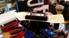
Bonus pics are showing a close up of the input stage and a close up of the 5R source degeneration of the 2SJ74BL jfets.
So far everything looks good, I got the frontend offset down to about 50mV, and with the VFETs installed the total output offset down to single digit mV.
There's one thing that bugs me a little, T5 (drain voltage of Q10) reads one volt less than T3 (drain voltage of Q7). I've tracked the issue down to the regs, and it seems that the voltage at the gate of Q8 differs by almost a Volt from the voltage at the gate of Q7. I still have to check if the other channel exhibits the same imbalance.
Bonus pics are showing a close up of the input stage and a close up of the 5R source degeneration of the 2SJ74BL jfets.
Attachments
Hi Rodeodave,
I the 3d scrulpture look...very nice.
The diff at T3 and T5. Is that just the inherent difference in Vgs between the
IRFP240 and IRFP9240 devices at at a given current level?
Cheers,
Dennis
I the 3d scrulpture look...very nice.
The diff at T3 and T5. Is that just the inherent difference in Vgs between the
IRFP240 and IRFP9240 devices at at a given current level?
Cheers,
Dennis
There's one thing that bugs me a little, T5 (drain voltage of Q10) reads one volt less than T3 (drain voltage of Q7). I've tracked the issue down to the regs, and it seems that the voltage at the gate of Q8 differs by almost a Volt from the voltage at the gate of Q7.
Check your resistor values around Q13 and Q14, R15 to R20.
Mr Pass,
I would like to thank you for your generous attitude towards the diy community, without which none of this would be possible.
Your gesture of offering access to your personal stash of VFETs, making the SONY VFET KIT available, is something unheard off. Wow!
Thank you Papa Pass.
I would like to thank you for your generous attitude towards the diy community, without which none of this would be possible.
Your gesture of offering access to your personal stash of VFETs, making the SONY VFET KIT available, is something unheard off. Wow!
Thank you Papa Pass.
Variac,
I would also like to thank you for all your hardwork bringing the SONY VFET KIT to light.
Thank you Variac.
I would also like to thank you for all your hardwork bringing the SONY VFET KIT to light.
Thank you Variac.
I've had an interesting weekend....There's one thing that bugs me a little....
@ Rodeodave
Just admire your boards and C3, 4, 5, 6 are 220 uF why not 47 uF ?
Kindest regards 🙂
47 uF charge quicker so you get vfet's bias in time.
Btw great build psu with serious noise filter.
🙂
Btw great build psu with serious noise filter.
🙂
Check your resistor values around Q13 and Q14, R15 to R20.
A quick update: The resistor values around the shunt regs seemed to be consistent enough in both channels. With the shunt regs themselves being the main suspect, I measured Vref (between R15/R17 to GND and between R16/R18 to the shunt's output) in both channels. While three of them measured the expected value of ~2.5V, the channel with the drain vintage inconsistency measured ~0.7V for Q13. After replacing Q13 everything now measures fine. Next step is putting everything together in the enclosure 🙂
@ Rodeodave
Just admire your boards and C3, 4, 5, 6 are 220 uF why not 47 uF ?
Kindest regards 🙂
I took the values from the Sony VFETs part 2 article and http://www.diyaudio.com/forums/blogs/tea-bag/352-sony-vfet-version-2-al-boards-build-blog.html with C3, 4, 5, 6 being 220uF and C1, 2 being 470uF.
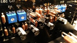
The attached pic is showing the newly biased channel with the replaced TL431 in action. I'm using a Caddock MP930 0R47 1% resistor as R32 since it's the only suitable part I've had on hands. 235mV drop would relate to 500mA through R32. Output offset is below one mV.
Attachments
- Home
- Amplifiers
- Pass Labs
- Sony vFET Amplifier Part 2