My suggestions:
- leave CCSs as they are
- change D5 and D6 to 20V
- connect D5/D6 to ground, instead diff pair emiters
- adjust R40 and R41 if necessary
You'll get better performance and much better PSRR.
- leave CCSs as they are
- change D5 and D6 to 20V
- connect D5/D6 to ground, instead diff pair emiters
- adjust R40 and R41 if necessary
You'll get better performance and much better PSRR.
No way. With D5/D6 to the ground we will lose the constant voltage on the input transistors. After that we will have a parasitic BC capacitance in action, which will be multiplied with the gain of the input stage. We will have Early effect too with common mode distortion.
So if you want an "upgrade" in the front stage, use of CRD's is the optimum solution or a CCS's in the place of the R40 and R41.
So if you want an "upgrade" in the front stage, use of CRD's is the optimum solution or a CCS's in the place of the R40 and R41.
No way. With D5/D6 to the ground we will lose the constant voltage on the input transistors. After that we will have a parasitic BC capacitance in action, which will be multiplied with the gain of the input stage. We will have Early effect too with common mode distortion.
So if you want an "upgrade" in the front stage, use of CRD's is the optimum solution or a CCS's in the place of the R40 and R41.
You are absolutely correct, with one exception. R40 and R41 cause much more common mode distortion that early effect. Probably if You drop all cascoding (around diff pair and CCS too), You'll get better performance.
Hi wojtek5001.
I am sorry to inform you that simulator do not give good results to your mods.
I get better results doing lots of mods and it become a new project.
Following you have simulation results. With wp in the end is your proposal. You can find my libs in this thread.
I wonder if Alexmm make PCB for my modified version.
Regards
Ronaldo
Attachments
Hi wojtek5001.
I am sorry to inform you that simulator do not give good results to your mods.
I get better results doing lots of mods and it become a new project.
Following you have simulation results. With wp in the end is your proposal. You can find my libs in this thread.
I wonder if Alexmm make PCB for my modified version.
Regards
Ronaldo
My suggestions was different, by the way. I've suggested simplification, by removing cascodes and so on, like in my schematic from my previous post. Additional CCS was proposed by someone else, and I agreed that it's good idea, but too much complications.
You can simplify but lose the essence... The input stage is not under negative feedback, so, it must be properly linearized. There will not be differences in the amplifier open loop gain perspective, but you will lose the input stage linearization.
From my point of view, the real and beneficial upgrade, it is the change R40 and R41 with a Curent Regulator Diode. The cost for this change it is 4x2$=8 maybe 10$. We can swap too the input stage transistors 2n5551 and 2n5401 with high beta and low noise BC550 and BC560.
From my point of view, the real and beneficial upgrade, it is the change R40 and R41 with a Curent Regulator Diode. The cost for this change it is 4x2$=8 maybe 10$. We can swap too the input stage transistors 2n5551 and 2n5401 with high beta and low noise BC550 and BC560.
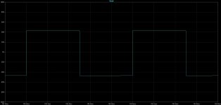
I went back to the drawing board and I pushed things even further. We can push the slew-rate and above in a safety margin. Phase margin 80 degrees, gain margin 16.5dB.
Attachments
Last edited:
great work
Hi Alex,
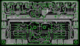
A very nice circuit board. Great work. I would like to use the circuit board. However, with 3 pairs of output transistors. I will transfer the board to Sprint layout.
Regards,
Gerd
Thank you greierasul .....
Have layout another PCB for the same schematic with OT in line ....not tested 🙂
I see ,no one interested in this circuit .....🙁 no comments .
Regards ,
Alex
Hi Alex,
A very nice circuit board. Great work. I would like to use the circuit board. However, with 3 pairs of output transistors. I will transfer the board to Sprint layout.
Regards,
Gerd
wojtek5001
You make a good new project with a bit better result using a low part count. It is the good thing of forum, we can change ideas to make a new general knowledge. My point is it - the knowledge.
Using schematic you can make your idea clear without any doubt.
I must agree with Greierasul, when you make any change in an amplifier project you change the amplifier essence and make a new project at your risk.
Another important point is simulator only give you a reference. In this template you only check one working point using an ideal power supply. It is not the real thing. You can make changes in this template and compare results to see what you gain and what you loose making changes. This is the idea of simulate.
Alexmm can give us real information concerning the project as he assembled the real amplifier
Chers
Ronaldo
Last edited:
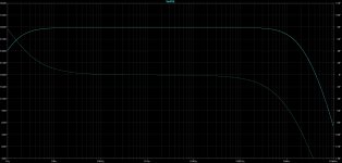
Please, have a look in this simulation.
It is the mixed proposal with an optimul zerner polarization current and a lower compensation resistor as proposed by Greierasul in early post.
It will take a while to finish 121 simulations but we can see the amplifier behavior in a large variation of voltage input and frequency.
The point is the variation of distortion in function of voltage level and frequency.
The distortion pointed is at 1Vpp and 10KHz. I use this as reference to compare designs
Regards
Ronaldo
Attachments
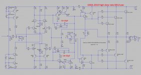
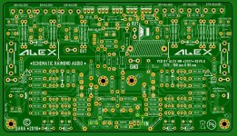
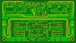
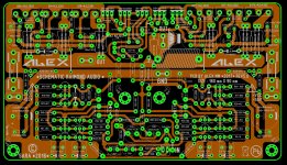
Schematic v.2 and PCB rev.5
PCB layout with 3 OT in line 😉 It's a beautiful, singing, amplifier ,I love it. 😀
Regards,Alex
PCB layout with 3 OT in line 😉 It's a beautiful, singing, amplifier ,I love it. 😀
Regards,Alex
Attachments
Last edited:
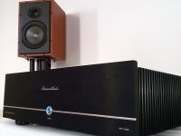
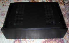
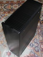
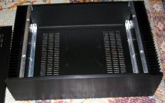
I agree,I have one...... 😀Now you need a housing for the amplifier , Alex. Why not like this...
Regards ,Alex
Attachments
excellent desined
V5 is looking better than V1.0 and better fitting in chasis ...lovely desined
PCB layout with 3 OT in line 😉 It's a beautiful, singing, amplifier ,I love it. 😀
Regards,Alex
V5 is looking better than V1.0 and better fitting in chasis ...lovely desined
Excellent!PCB layout with 3 OT in line 😉 It's a beautiful, singing, amplifier ,I love it. 😀
Regards,Alex
Can you share pcb files?
Hi , yes I can , here are the files 😉Excellent!
Can you share pcb files?
Regards,Alex
Attachments
Good you are back, Alex!
Every new pcb brings a smile to all of us! I always print it off in colour then walk to my local café for a careful examination with strong coffee........ always a pleasure.
Beautiful work, congratulations to our resident da Vinci........
Ciao,
Hugh
Every new pcb brings a smile to all of us! I always print it off in colour then walk to my local café for a careful examination with strong coffee........ always a pleasure.
Beautiful work, congratulations to our resident da Vinci........
Ciao,
Hugh
- Home
- Amplifiers
- Solid State
- SARA-2016