Not a different topic. I am asking if I have misunderstood the phase of the correction that gets applied to the _IN node.I agree with the rest, with addition that in some cases, some other (better?) places of offset control may be found - for example, in the design with symmetric CCSs feeding the diamond, great thing to control is the CCSs' currents balance (servo moves it up or down, zeroing-out DC at the output).
i.e. another misunderstanding of the way AC electronics works.
My list of misunderstood topics keeps growing !
So,offset controller is wrong designed.
Likely if you were to see the whole schematic, OS would have a voltage applied to the NFB signal in the simulation to test the servo. The initial offset needs to be coming from somewhere.
If you look at the design, the input transistors would balance out if a pot was installed between R8, R9 and R10 to trim offset.
Not a different topic. I am asking if I have misunderstood the phase of the correction that gets applied to the -IN node.I agree with the rest, with addition that in some cases, some other (better?) places of offset control may be found - for example, in the design with symmetric CCSs feeding the diamond, great thing to control is the CCSs' currents balance (servo moves it up or down, zeroing-out DC at the output).
i.e. another misunderstanding of the way AC electronics works.
My list of misunderstood topics keeps growing !
.
My list of misunderstood topics keeps growing !
This is what keeps the hobby interesting!
This already done.(servo disconnected).No, there is something else that is causing the need for this excessively high correction signal. Disconnect the servo and investigate.
Offset without servo is 2.5mV.
Attachments
The original sch in post1523 is correct, except for that high voltage and the need for 1:1 resistors to apply that big correction.Likely if you were to see the whole schematic, OS would have a voltage applied to the NFB signal in the simulation to test the servo. The initial offset needs to be coming from somewhere.
If you look at the design, the input transistors would balance out if a pot was installed between R8, R9 and R10 to trim offset.
The revised values shown in post1553 is not good. It appears to have fudged component values without curing the cause that requires the high correction voltage.
what are the voltages at those nodes and what are the voltages across those resistors.This already done.(servo disconnected).
Offset without servo is 2.5mV.
This already done.(servo disconnected).
Offset without servo is 2.5mV.
Can you check offset voltage through a whole startup cycle? Does it start excessively high, then drop?
I think that is low from the start but i will check this again.Can you check offset voltage through a whole startup cycle? Does it start excessively high, then drop?
I think that is low from the start but i will check this again.
That's interesting! Performance is better without the servo. This would tell us to look at the servo instead of the rest of the circuit.
Yes Jeff,i will post all the distortion measurements, without servo version,soon.Big difference!😱That's interesting! Performance is better without the servo. This would tell us to look at the servo instead of the rest of the circuit.
This already done.(servo disconnected).
Offset without servo is 2.5mV.
But that means - the servo output must be somewhere in the 10-th millivolts order - correction required is low.
Yes i see,but what is Wrong?🙁But that means - the servo output must be somewhere in the 10-th millivolts order - correction required is low.
Let's go!
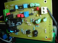
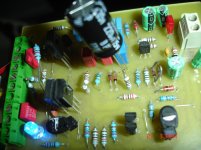
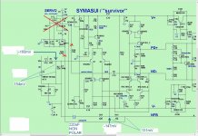
No servo Symasui Survivor IPS+NS OPS
No servo Symasui Survivor IPS+NS OPS
Attachments

Last edited:
AnderewT that is.What are the voltages at those nodes and across those resistors?
Jeff, without servo offset goes to 2.5mV instantly!
Attachments

Last edited:
I Think so😉It looks like a great amplifier as is. No real need for the servo.
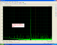
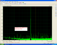
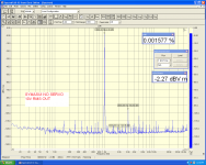
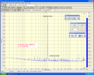
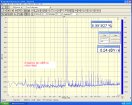
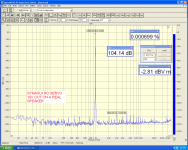
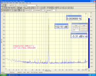
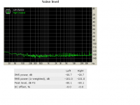
In these two measurements a real 3 way speaker was used as load.
The last one without any load.
Attachments

Last edited:
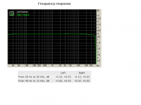
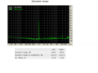
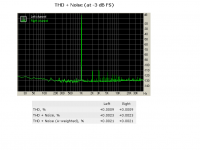
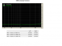
Testing Symasui Survivor+NS using RMAA
RMAA test Report.
RMAA test Report.
Attachments


Last edited:
-160mVdc at the input node cannot be right.
It should be a +ve voltage, because the base current comes from the +ve supply through R2 to Signal Ground and thence through R3 to Power Ground.
Check the voltage @ R3, looks like it is ~+3mVdc reference the Power Ground and 0.0mVdc reference the Signal Ground.
3mV indicates 300uA flowing from Signal Ground to Power Ground. This could be adjusted to be quite a bit less, but I don't know how it varies with temperature. Worth checking when cold, warm, hot.
Same error for the -147mVdc voltage.
Last edited:
- Home
- Amplifiers
- Solid State
- Revisiting some "old" ideas from 1970's - IPS, OPS