Thanks for clearing connection C7 and some things more last days here.
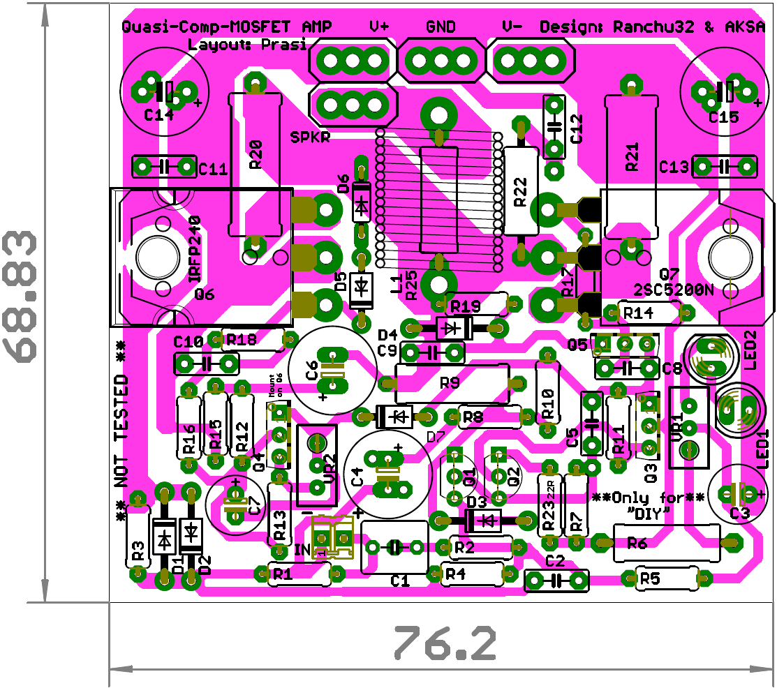
Dacz- same thought like X, nice board and all values are printed to part- nice.
There was any debate about R20/21- it is more safe way to use 0,33R- best compromise-
Ranchu tells us.
Cheers Bangla.
Dacz- same thought like X, nice board and all values are printed to part- nice.
There was any debate about R20/21- it is more safe way to use 0,33R- best compromise-
Ranchu tells us.
Cheers Bangla.
Why THD20k /1W is slightly higher than THD20k/ 50W? The circuit need higher bias?
You've noticed that quite well. It is not only for this version(tpc + nested), but it's characteristic for all version I simulated. Only explanation I have, this is characteristic for this type of OPS. Higher bias does not change that, and it's not only at 20 kHz.
Thank YouOnly explanation I have, this is characteristic for this type of OPS. Higher bias does not change that, and it's not only at 20 kHz.

What is the efficiency of this intriguing little guy? Also, has a BOM been posted? Don't remember seeing one but maybe I just ignored it accidentally.
2N5401/2N5551 from prasi rev2
Hi, Thats a very nice layout. 2n5401/5551 are not from my layout. they were added later as per suggestion by AKSA for XRK. xrk twisted the legs to use them on his PCB. I havent yet revised the layout to include them+other changes as per AKSA's recent sch.
reg
Prasi
edit: consensus here is not to use 2sc5200 at 42 V, better to substitute it with onsemi 200W MJL at that voltage
Last edited:
Guys, I wouldn't obsess over the choice of input transistor. The KSA992 I specified works well; Hugh suggested the 2N5401 as an alternative to someone who couldn't readily source the KSA. I've used both in different project and can't distinguish any difference. I wouldn't obsess over this!
42V is about the limit for the 2SC5200 and really only suitable for 8 ohm and relatively benign loads in my experience.
42V is about the limit for the 2SC5200 and really only suitable for 8 ohm and relatively benign loads in my experience.
Guys, I wouldn't obsess over the choice of input transistor. The KSA992 I specified works well; Hugh suggested the 2N5401 as an alternative to someone who couldn't readily source the KSA. I've used both in different project and can't distinguish any difference. I wouldn't obsess over this!
42V is about the limit for the 2SC5200 and really only suitable for 8 ohm and relatively benign loads in my experience.
ok, thanks for the info.
reg
Prasi
The 1943/5200 has very poor SOA at higher voltages........................
42V is about the limit for the 2SC5200 and really only suitable for 8 ohm and relatively benign loads in my experience.
They are more suitable for lower voltage amplifiers.
That makes the 5200 MORE suited to 4ohms amplifiers, than to high power 8ohms amplifiers.
I have suggested in the past that you should not use 1943/5200 at over ±55Vdc (quiescent supply voltage).
42Vdc and 50Vdc can both be made to work if you take account of the temperature de-rated SOA appropriately.
ClassH and ClassG are a different ballgame and I don't have any data for those types of amplifiers.
Last edited:
What is the efficiency of this intriguing little guy? Also, has a BOM been posted? Don't remember seeing one but maybe I just ignored it accidentally.
It's still evolving as an amp design - although values are much more stable now. I think you have to work off the schematic for the BOM. It's such a low parts count amp that it's not an issue. The thing to note are a few of the resistors need to be higher power rated (as noted).
It's still evolving as an amp design - although values are much more stable now. I think you have to work off the schematic for the BOM. It's such a low parts count amp that it's not an issue. The thing to note are a few of the resistors need to be higher power rated (as noted).
X, if you get time, can you take the excel i posted, enter your values +schema link+layout link and re-post here for convenience of others? same request for Terry also for his second build if completed.
The 1943/5200 has very poor SOA at higher voltages.
They are more suitable for lower voltage amplifiers.
That makes the 5200 MORE suited to 4ohms amplifiers, than to high power 8ohms amplifiers.
I have suggested in the past that you should not use 1943/5200 at over ±55Vdc (quiescent supply voltage).
42Vdc and 50Vdc can both be made to work if you take account of the temperature de-rated SOA appropriately.
ClassH and ClassG are a different ballgame and I don't have any data for those types of amplifiers.
Andrew, regardless of what is implied in the Toshiba datasheet, it has been my practical experience with these parts that they are prone to failure with >45V rails, particularly when driving 4R (even dummy, pure resistor) loads. I stand by my comment that a single 5200 from 42V rails, in a design like this, driving a 4R speaker, is a ticking time bomb.
I'd also point out that the "1943/5200" part numbers are thrown around generically here, and I'm doubtful that would-be builders are always referring to and sourcing the original devices. There appears to be a large number of second source, similarly numbered and outright fake parts floating around that do not necessarily meet the Toshiba specs, so it seems prudent to err on the side of caution when making recommendations.
42Vdc and 50Vdc can both be made to work if you take account of the temperature de-rated SOA appropriately.
A single pair of 150W devices has a total cold Pdiss of 300W. That gives a reliable 50W maximum output.Andrew, regardless of what is implied in the Toshiba datasheet, it has been my practical experience with these parts that they are prone to failure with >45V rails, particularly when driving 4R (even dummy, pure resistor) loads. I stand by my comment that a single 5200 from 42V rails, in a design like this, driving a 4R speaker, is a ticking time bomb...................
If you want to use 1943/5200 on ±42Vdc with a 4ohms loading, expect around 120W to 160W of maximum output. That would require at least 2pairs of 5200 devices.
And for ±50Vdc you would need at least 3pairs to take account of the temperature de-rated SOA.
Trying to use 1pair @ ±42Vdc to drive a 4ohms load is asking for unreliability.
Is 22-24Vdc for 4ohm speakers too little for this? I'm thinking of attempting a battery powered portable version. It's pretty weird, I know, but is it entirely idiotic?
Last edited:
X, if you get time, can you take the excel i posted, enter your values +schema link+layout link and re-post here for convenience of others? same request for Terry also for his second build if completed.
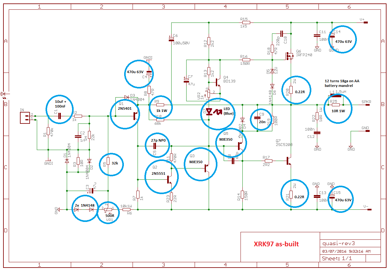
Here is my schematic as-built, many of the substitutions were simply result of using what I have on hand. The key functional substitutions are:
blue LED, 2x 2N4148's, R9=1k 1W, R5=33k (32k as built). The capacitors were simply use of what I had on hand.
Attachments
Last edited:
Here is my schematic as-built, many of the substitutions were simply result of using what I have on hand. The key functional substitutions are:
blue LED, 2x 2N4148's, R9=1k 1W, R5=33k (32k as built). The capacitors were simply use of what I had on hand.
thats nice and clear, thanks!
reg
prasi
can please verify electrolytics voltages?
If you are using +-42V rails you should be fine with 50V caps. You don't have the blue LED connected right. It should connect to the same place as Zener but reversed.
Last edited:
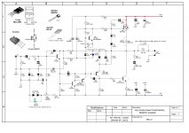
Dacz,
You have set R7 at 680R and this is in error. It has been usually set at 10R, but in fact someone here, maybe Terry?, who discussed it should be zero, that is, leave it out altogether. C4 has also been addressed by Thiago, who felt the bass was superior with 1000uF rather than 470uF. From the design POV, deleting R7 increases the loop gain of the amp by quite a margin, but the global feedback is set by the ratio of R10 and R9, 68k/1k8, which defines the global negative feedback as 37.7, which around 31dB.
You describe Q5 as the phase inverter; moving left to right, it's actually a VAS buffer transistor (impedance device) and might be redesignated as Q3; and your Q5 is a phase inverter and might be designated Q5.
Otherwise, your drafting is very clear and well done!
Hugh
Last edited:
can please verify electrolytics voltages?
Error: alternative (to the Zener) blue LED on your diagram is connected to the output, instead of Q4 emitter.
- Home
- Amplifiers
- Solid State
- Very simple quasi complimentary MOSFET amplifier