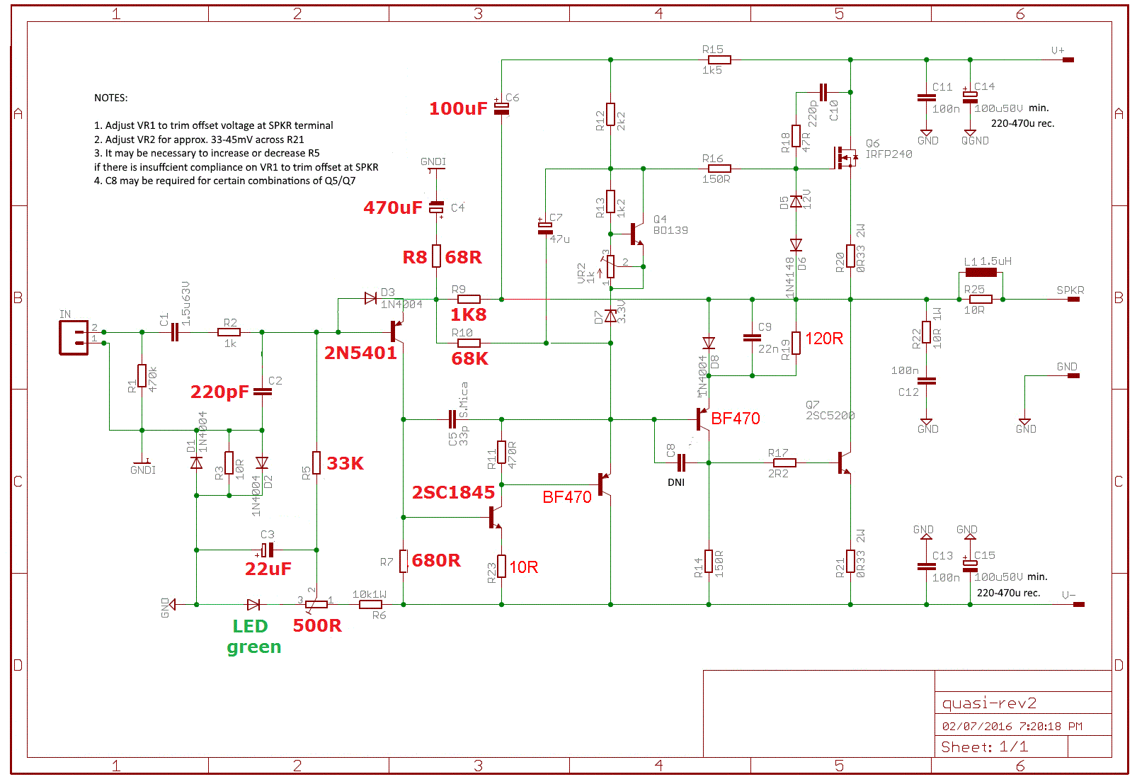
Which side of D7 is the connection to C7? For most of this thread it the negative side of C7 has connected to the cathode side of D7 (the Prasi layout reflects this). In post 988 it changed to the anode side of D7. Does this make a difference? (first noted by Bangla H in post 1048).
Steve.
Steve.
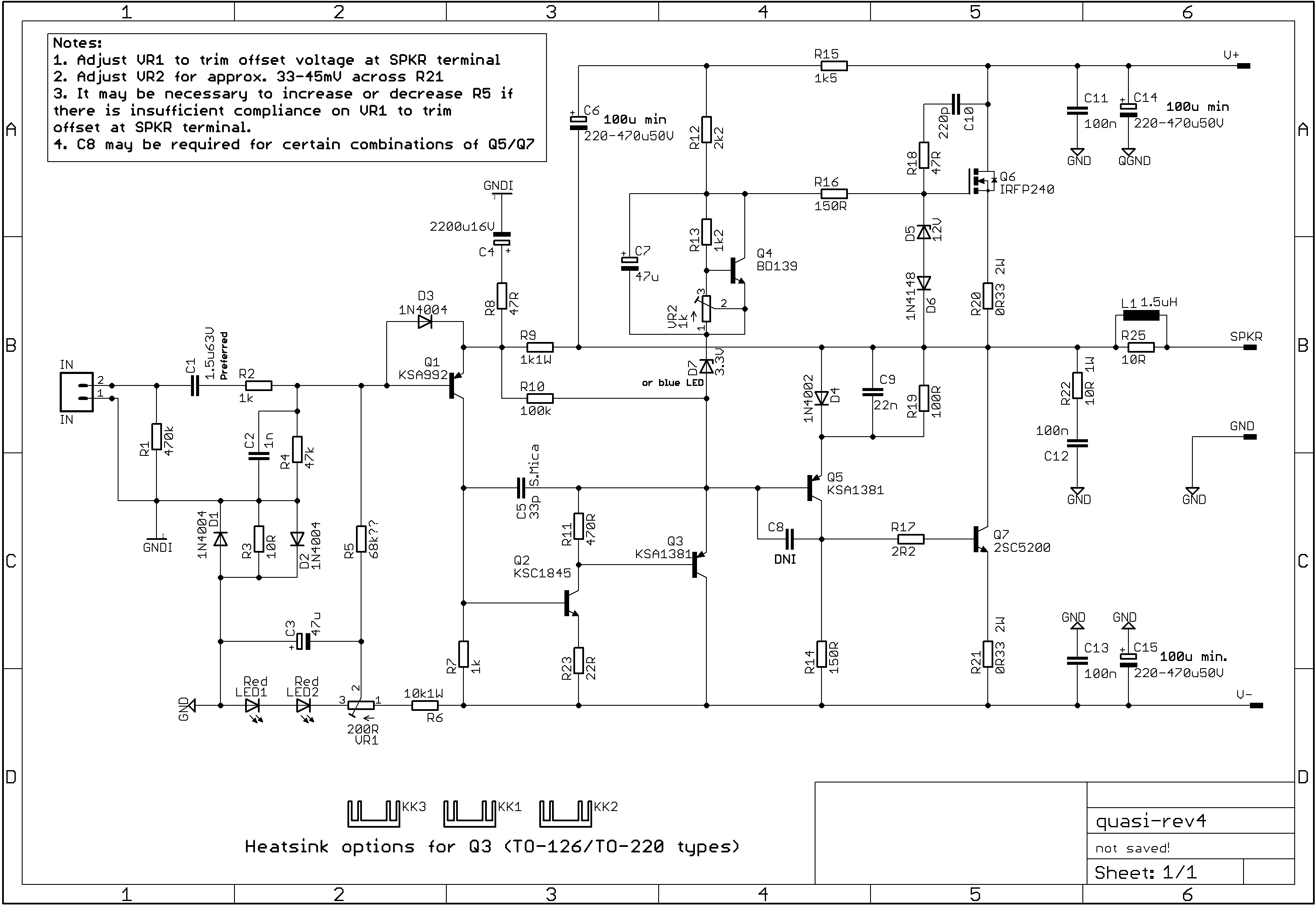
Are we going with this as the latest schematic?
The Prasi boards were made according to this schematic which has D7 below the point where C7 ties into the bias control path. The 68k resistor is also connected in a different place. Is this a difference between Prasi's board and Thimios' and Thiamogo's boards? They won't behave the same I don't think.
Does this change things? If D7 is a blue LED then cathode needs to go opposite end of Zener to allow flow.
I wonder if this is why Terry ran out of bias adjustment range because boards are different and when we refer to changes in resistors - it affects the two designs differently.
Last edited:
I will be happy to put them side by side on the A/B setup tomorrow is that will help you.hugh,
yes, I think 1000uF can be perfect , I'll try .
Terry , if you can compare with FX8 I would be happy .
Regards
Thiago
Blessings, Terry
Last edited:
Bias voltage required is Vgs of Q6+ drop on R20 + drop on R19+ Vbe Q5 ( BF470)
which is about 4.633 V
So voltage generated by bias circuit around Q4 should be 4.633-V zener
= 4.633- 3.3V = 1.333 V.
If you use a blue LED ( 2V drop) this voltage would be 2.633 volts . Temp comp would change as Q4's contribution changes in the total voltage.So compensating voltage here would have a greater effect on bias control.
C7 shorts out ac across the bias voltage. By connecting it to the VR2 and D7 junction it leaves out the zener and the zener's dynamic resistance of a few ohms will come in series in the bias voltage circuit. Not a dc problem but could inject some ac into the bias voltage. It's up to you to see if that matters audibly.
Quasi Rev 2 circuit seems to be the more correct one.
Nobody answered why the diode D3 is at the input transistor base emitter. Protection for bad clipping or a dead short at the output ?
Also why R10 was used (68K). It provides additional internal feedback dc and ac . Is that required for stability of either dc or ac ? DC seems unlikely as it's swamped by the current through the real feedback resistor R9 ( 1.8K ). Did anyone simulate this and remove R10 ? Under normal condition diode D3 should have no effect.
Does anyone have an .asc file .
Thanks.
Last edited:
hugh,
yes, I think 1000uF can be perfect , I'll try .
Terry , if you can compare with FX8 I would be happy .
Regards
Thiago
I started a new thread where you can listen (audition) this amp as compared to FX8 Bimo, FH9, JFET Circlophone, and VHEX+ amps.
http://www.diyaudio.com/forums/soli...very-simple-quasi-mosfet-amp.html#post4797058
Ashok, I think AKSA already explained, some post earlier, why the nested feedback, that allows for mild GNF...
I start drawing a .asc, but lack of a model for de IRPF part, nor the BF470, stop me
I start drawing a .asc, but lack of a model for de IRPF part, nor the BF470, stop me
Last edited:
Points of Contention
Hi Spind, and Ashok,
D7 is a voltage reference. If you use a zener, then the cathode is connected to the Vbe multiplier, Q4, but if you use a blue LED then to pass current you must have the anode connecting to the Vbe multiplier.
Hi Spind, and Ashok,
D7 is a voltage reference. If you use a zener, then the cathode is connected to the Vbe multiplier, Q4, but if you use a blue LED then to pass current you must have the anode connecting to the Vbe multiplier.
Bias voltage required is Vgs of Q6+ drop on R20 + drop on R19+ Vbe Q5 ( BF470)
which is about 4.633 V
So voltage generated by bias circuit around Q4 should be 4.633-V zener
= 4.633- 3.3V = 1.333 V.
If you use a blue LED ( 2V drop) this voltage would be 2.633 volts. Temp comp would change as Q4's contribution changes in the total voltage. So compensating voltage here would have a greater effect on bias control. /QUOTE]
Yes, these figures look correct from my end as well. A blue LED does not have a zero tempco like 3.3V zener, and in fact the additional voltage across Q4 with a blue LED would be 2V, compared to across 1.33V when using the 3.3V zener, which has close to zero tempco and which then throws all the compensation onto the Vbe multiplier, Q4. I think the zener is the better way, actually, since the tempco should match the nmos and the lightly driven BF470phase inverter which should be Q5 (but not designated, a minor flaw!). I would say that while the blue LED gets it going nicely, the best option is the 3.3V zener because with 1.33V across Q4 we have around two pn junctions temperature compensated, almost ideal. Result: a better control of quiescent. Nonetheless if you over compensate any amp the result is that the hotter it gets the lower the quiescent drops, and if you start out at 125mA, the recommended, when it gets really hot and drops the quiescent drops to about 40-50mA. Furthermore, when you turn it on, it runs a higher quiescent, and then after 20 minutes running it comes quite a bit, and this helps warm the amp up so you achieve best sound a little quicker. Clearly this way the amp is failsafe, as compared to one which is precisely compensated thermally and sits rock stable at 125mA at any temperature. If you under compensate, even with a few degrees/mA, the amp will definitely fail sooner or later with thermal runaway. Better to have more, than less!
C7 shorts out ac across the bias voltage. By connecting it to the VR2 and D7 junction it leaves out the zener and the zener's dynamic resistance of a few ohms will come in series in the bias voltage circuit. Not a dc problem but could inject some ac into the bias voltage. It's up to you to see if that matters audibly.
Quasi Rev 2 circuit seems to be the more correct one.
Yes, I picked this up too and C7 should include the Vbe multiplier AND the Zener. Besides, it helps move charge into and out of the mosfet from the very low emitter of the VAS buffer, the BF470. This has issues for slew rate, too.
Nobody answered why the diode D3 is at the input transistor base emitter. Protection for bad clipping or a dead short at the output ?
Good call - this protect the pn junction if a fast positive pulse enters the base which exceeds 5V more than the emitter point. This otherwise would take out the input transistor because base/emitter junctions are unreasonably sensitive to more than 5V of reverse bias. Put another way, if 5V HIGHER at the base than the emitter on a pnp will destroy the transistor, so since we have a minimally protected input to Q1 we must practise safe sex as the wise engineer would always say...... This junction is also vulnerable from the emitter, since it is attached to the output speaker with heavy voltage and drive. If the speaker output drops more than 5V (positive or negative, in fact) wrt the input base, again, the device is destroyed. So this resistor maintains safe operation. In the clip situation, as Ashok mentions, all sorts of voltages fly around an amp and you must guard against these malevolent energies from destroying the input stage; the classic situation is a short, of course, but there are also issues such as speaker reactances, or a ham-fisted fellow putting 240Vac into the amp. It may not protect ALL the transistors only, but hey, these things do happen...... I have found customers are very creative this way.
Also why R10 was used (68K). It provides additional internal feedback dc and ac . Is that required for stability of either dc or ac ? DC seems unlikely as it's swamped by the current through the real feedback resistor R9 ( 1.8K ). Did anyone simulate this and remove R10 ? Under normal condition diode D3 should have no effect.
It does improve stability because it reduces the global feedback to 31.5dB rather than the usual 46dB with conventional, full global feedback. The lag compensation can be relaxed to a degree; in this amp will be quite stable with 22pF in C5. We suggest 33pF With full global you could use around 40pF or more. I can see Ashok's concern about this resistor, however, consider this:
R10 68k is nested feedback, which reduces the loop gain of the amp as a whole. This brings more distortion, but only low order. If you examine the H7 and beyond, you find that these harmonics are ALL suppressed.
If you build this, Ashok, and I hope you do, put in this resistor so you can remove its effect, and compare before and after. I cannot convince you, but I can exhort you to do it. If you like it, you will change your views about THD and entire cabal of high end nonsense. If you do not like it, you will be convinced that I'm a crazy Australian...... there is the challenge, Sire!!
Does anyone have an .asc file
Cheers,
Hugh
Attachments
It does improve stability because it reduces the global feedback to 31.5dB rather than the usual 46dB with conventional, full global feedback. The lag compensation can be relaxed to a degree; in this amp will be quite stable with 22pF in C5. We suggest 33pF With full global you could use around 40pF or more. I can see Ashok's concern about this resistor, however, consider this:
R10 68k is nested feedback, which reduces the loop gain of the amp as a whole. This brings more distortion, but only low order. If you examine the H7 and beyond, you find that these harmonics are ALL suppressed.
If you build this, Ashok, and I hope you do, put in this resistor so you can remove its effect, and compare before and after. I cannot convince you, but I can exhort you to do it. If you like it, you will change your views about THD and entire cabal of high end nonsense. If you do not like it, you will be convinced that I'm a crazy Australian...... there is the challenge, Sire!!
Cheers,
Hugh
Here are mine .asc files.
In my opinion nested feedback does not improve stability significantly as the compensation slope stays the same.
I simulated MC with and without nested feedback and only what I noticed is more increased second harmonic comparable to other harmonics with nested feedback in situ, and could be what give to someone more euphonic sound.
Damir
Attachments
Hi Hugh,
Thanks a ton for the superb explanation and the .asc file...Ranchu too ! You bet I'll try the circuit with R10 and without. DIY is no fun without a 'what if situation' !
Will take a while....I'm moving home. But will do some preliminary work.
Damir: Thanks for your files. I have something more to work on when the 'lab' is down !
Cheers.
Last edited:
Damir,
I will not argue about the stability; to be honest, this is easy to achieve with this amp with either lag comp, or lag shunt, or TMC. However, rather than a simple increase in euphonic H2 it has another quality, even at very low levels of nested fb, which I would call spatiality.
This cannot be measured in usual methods, but it can be heard strikingly with depth of image, something you notice strikingly with tube amplifiers.
Thank you for your post!
Ciao,
Hugh
Hi Hugh .
Should I worry about changing the C7 position?
My PCB do not bind to C7 in anode ZENER.
Thanks
Thiago
Should I worry about changing the C7 position?
My PCB do not bind to C7 in anode ZENER.
Thanks
Thiago
I'm not sure what the effect sonically would be, Thiago, you might try it on your pcb and a listening session - but as Damir suggested the dynamic impedance of the zener would be little different to including the pcb in C7; it may be possible that it might not have any difference, although it is very clear to me that the difference would be H2 only, probably not a bad thing.......
Thanks for the post,
Hugh
Thanks for the post,
Hugh
Damir,
I will not argue about the stability; to be honest, this is easy to achieve with this amp with either lag comp, or lag shunt, or TMC. However, rather than a simple increase in euphonic H2 it has another quality, even at very low levels of nested fb, which I would call spatiality.
This cannot be measured in usual methods, but it can be heard strikingly with depth of image, something you notice strikingly with tube amplifiers.
Thank you for your post!
Ciao,
Hugh
Hugh,
I don't argue, just observation taken from the simulation. Of course final judgement is listening and I haven' done that.
Ciao, Damir
Damir,
I beat a drum for nested - I started building amps with nested fb and low global nfb ten years ago and I'm a convert despite the higher THD. I was so concerned with this THD issue that I begun to investigate the FFT figures.
Then I noticed tube amps, comments from JLH, Pass and Hansen and realised they knew a lot more than they were saying....
Like many wacky ideas you have to listen for yourself and trust your own ears. Only a few do this of course but since audio memory is very fleeting only an AB test definitively proves it.
Hugh
However, rather than a simple increase in euphonic H2 it has another quality, even at very low levels of nested fb, which I would call spatiality.
Hugh,
Can spatiality be heard with a mono setup? Probably not - so for me to capture that in my sound clips would require a stereo setup and stereo mics, no?
Hugh, two questions; why persist with BF470 in your Sims? They are no longer available.
Can rail voltage be increased to 42 volts and output pair doubled for higher power into 4 ohm loads?
Can rail voltage be increased to 42 volts and output pair doubled for higher power into 4 ohm loads?
XRK,
Yes you would need both channels to hear depth of image!
However you do have two channels now?
Samuel,
I originally used KSA1381 for design and prototyping but any fast, low Cobb TO126 flatpack which can cope with 200mA is fine. Because one builder could not find it locally and had the BF470 on hand one guy (Prasi?) changed the schematic and I went with it. This amp with IRFP/C5200 output stage will work to 42V rails (30Vac supply) but not for 4R loads.
HD
Last edited:
- Home
- Amplifiers
- Solid State
- Very simple quasi complimentary MOSFET amplifier