Hi Hugh,putting a second resistor(2K2) in parallel to 1K2 (result is 776R)I endet up with 0.042V on the emitter resistor(0.33R) when trimmer 1K is at max resistance,do you think that this new resistor must be even lower?
Something wrong. What voltage is across the 3.3V zener, the Vbe multiplier C to E, and how much voltage from nmos to base of pnp phase inverter?
Hugh
V across zener= 3.45vSomething wrong. What voltage is across the 3.3V zener, the Vbe multiplier C to E, and how much voltage from nmos to base of pnp phase inverter?
Hugh
Vce mult=1.1V
Vgate V base Q5=4.8V
Keep in mind that is the channel where D8,C9 are omitted and R19 is a link
Thanks.
Last edited:
Ah, that is OK.....
You should have about 130mA now with 42mV across -0.33?
Thimios, without the R/C/diode between emitter of inverting transistor and the output node you will have very tetchy adjustment; it will be very sensitive.
One of the advantage of the Baxandall network is that it makes adjustment easy but particularly it means the upper device, the nmos, remains on right through the waveform, delivering a kind of semi-class A for this amp. The quasi turns on and off, but the nmos is always on. This reduces odd order distortion, worth having.
Ciao,
Hugh
Hi Guillermo,
Well, in my opinion, but I like to make the amp easy to set up and I particularly like to ensure that the upper device, the nmos, remains ON through the full cycle. This minimises the odd order distortion since one of the devices never turns off, but of course without the R/C/diode network (the Baxandall cell) the amp will work just fine. If you want to reduce the parts count, then this is fine, but it's a manufacturing decision. For DIY where 20c of parts is not required then it seems sensible to put it in and all the three parts, R, C and diode, are needed.
Cheers,
Hugh
Hugh.
It is understood perfectly. Thank you very much for your contribution to help understand how it works out this particular output stage, NMOS - NPN.
Regards
Guillermo
It is understood perfectly. Thank you very much for your contribution to help understand how it works out this particular output stage, NMOS - NPN.
Regards
Guillermo
Yes,i have 42mV across 0.33 but when the trimmer(idle current adj.) VR2 is at his end position.Ah, that is OK.....
You should have about 130mA now with 42mV across -0.33?
Thimios, without the R/C/diode between emitter of inverting transistor and the output node you will have very tetchy adjustment; it will be very sensitive.
One of the advantage of the Baxandall network is that it makes adjustment easy but particularly it means the upper device, the nmos, remains on right through the waveform, delivering a kind of semi-class A for this amp. The quasi turns on and off, but the nmos is always on. This reduces odd order distortion, worth having.
Ciao,
Hugh
The other channel is.
Vzener=2.87V
VceTR5=1.9V
Very late for edit🙁Yes,i have 42mV across 0.33 but when the trimmer(idle current adj.) VR2 is at his end position.
The other channel is.
Vzener=2.87V
VceTR5=1.9V
Vzener=2.87V
Vce Q4=1.9V
Thimios,
I really think you should insert the Baxandall R/C/diode. This will make the quiescent far less sensitive, deliver more adjustment range and maintain the upper mosfet in the on-state for almost all of the output waveform.
Drat, I'd hope these three components could be dispensed with, but apparently not......
Ciao,
Hugh
Agreed. Thimios, thanks for trying out this experiment at my request. Another member suggested the Bax components weren't useful with this "hybrid" quasi output stage but I didn't anticipate these problems with bias setting.
I think its time to call it a day and consider the schematic for the first board thimios built the final version. I have a few other ideas I'd like to investigate, but that's another project, for another thread...
I think its time to call it a day and consider the schematic for the first board thimios built the final version. I have a few other ideas I'd like to investigate, but that's another project, for another thread...
Double checked.
When omitted these parts on the first channel i have the same problem.
So the recommendation is reinstalling these?
BTW what is the ideal power supply voltage?
When omitted these parts on the first channel i have the same problem.
So the recommendation is reinstalling these?
BTW what is the ideal power supply voltage?
Last edited:
Double checked.
When omitted these parts on the first channel i have the same problem.
So the recommendation is reinstalling these?
I would say yes. many people waiting to build this one😀😀. + waiting to read your impression in stereo mode
 .
.reg
Prasi
Yes, thimios, you should reinstall these components on both boards.
Hugh and I will be most interested to hear your listening report once you've had a chance to audition in stereo.
Hugh and I will be most interested to hear your listening report once you've had a chance to audition in stereo.
Yes Prasi and Ranchu i know🙂I would say yes. many people waiting to build this one😀😀. + waiting to read your impression in stereo mode
reg
Prasi
When everything is ok i will come back with listening details.
I will take this at home where me and my wife would listen to this carefully
Stay tuned!
Last edited:
Yes, Thimios, but you need to ensure that when you set the appropriate quiescent (somewhere between 100mA and 140mA, as you wish) at idle there is:
1. majority of current is passed through the Baxandall 100R resistor, and
2. a small current is passed through the Baxandall diode.
This removes the diode switching from the full waveform since the Bax diode is always ON.
This fine detail leverages the benefits of this network. To give you some idea:
Total collector current from the inverter transistor might be 8.5mA
Current through resistor might be 6mA
Current through diode might be 2.5mA
Generally you need to make the Bax resistor much smaller than the base to negative rail resistor. 100R v. 150R is a good ratio assuming the beta of the quasi output device is at least 80.
Cheers,
Hugh
Last edited:
Ok understood.😉Yes, Thimios, but you need to ensure that when you set the appropriate quiescent (somewhere between 100mA and 140mA, as you wish) at idle there is:
1. majority of current is passed through the Baxandall 100R resistor, and
2. a small current is passed through the Baxandall diode.
This removes the diode switching from the full waveform since the Bax diode is always ON.
This fine detail leverages the benefits of this network. To give you some idea:
Total collector current from the inverter transistor might be 8.5mA
Current through resistor might be 6mA
Current through diode might be 2.5mA
Generally you need to make the Bax resistor much smaller than the base to negative rail resistor. 100R v. 150R is a good ratio assuming the beta of the quasi output device is at least 80.
Cheers,
Hugh
What about ideal power supply voltage?
Hallo Ranchu and Prasi.
I also would etch your PCB, but the newer printer works so bad and i will not spent
money to new one- so i ordered, thanks your shared Files.
To Ranchu and you prasi, Thimios too and other i only can congrat to your creativity.
I am and Patrick, i hope also, are one the way to build, if boards received.
At moment i print the schematic and look wich parts are needed and reread where i must have attention.
So looking forward to Thimios Stereo impressions.?
Cheers Bangla.
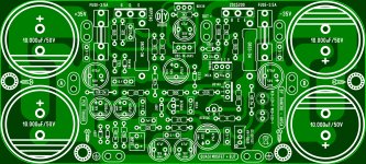
D8,C9,R19 back in position.
Now the Vbe multiplier is in normal conditions.
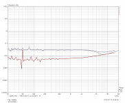
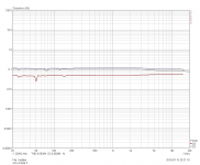
Trying to figure the distortion graph i see that one channel have a lower distortion than other. Same idle current,same offset,same levels,same power supply.
Duple checked.
Is this as a matter of transistors hfe ?
Now the Vbe multiplier is in normal conditions.
Trying to figure the distortion graph i see that one channel have a lower distortion than other. Same idle current,same offset,same levels,same power supply.
Duple checked.
Is this as a matter of transistors hfe ?
Attachments
Last edited:
Ok understood.😉
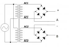
What about ideal power supply voltage?
Between 40-45V is about the limit for the 2SC5200. I run mine on 35V rails and it sounds great 😀
- Home
- Amplifiers
- Solid State
- Very simple quasi complimentary MOSFET amplifier