When I was a boy (now I’m 47), father some time said me that “se puede obtener buena calidad de un AM” (It is possible to get good audio quality from an AM receiver).
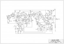
This tuner has been designed having in mind this idea, and an animus or spirit of to experiment some own ideas that I previously had in mind, and never before tested (by me) in a real circuit. Also, I used in it, materials recovered from the box of old stuff, most of them has been kept unused for more than a decade.
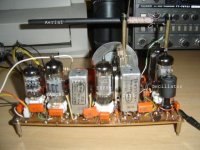
The first thing that I wanted to test, is an AM receiver with a RF amplifier stage, using a remote cutoff pentode, with the ferrite rod antenna (aerial) directly wired to the signal grid. Looking into my stock of tubes, I found an EF89 for the stage.
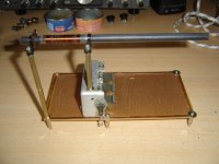
The gang condenser (G in the schematic) is triple equal sections made with brass sheets, at both stator and rotor plates, rescued from any Philips radio receiver.
The antenna (L1), the RF inter stage transformer and the oscillator coil has been designed following what is suggested in the Langford-Smith’s (LS) "Radiotron" book. The antenna I used is a rod saved from a discarded transistor radio, but rewind completely for this purpose using Litz wire, the last recovered from the inductor in wasted electronic ballast for fluorescent lamps. As I lack of characteristics or data sheets of the ferrites employed, a test coil has been made in each of them, and tested with a RLC digital meter.
RF transformer (L2) and oscillator coils (L3) use the same wire, but for them, I recycled the bobbin, the core and the magnetic shield from PC monitor horizontal width coil control.
The choused converter tube is an ECH81, the signal grid of the hexode is tied to the RF tuned transformer, and the injection grid wired together with the oscillator, which has the form of a tuned-grid tickler-coil (or Armstrong) oscillator, with series feed in both windings.
The RF and antenna coils have been calculated as is suggested in chapter 23 of the LS's book. Oscillator coil, padder and trimmers make use of the formulae at chapters 24 and 25, mainly from Section 3 of the last, in which the tracking between RF and oscillator method is described.
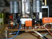
IF section follows those described in Chapter 26, but making use of standard double-tuned mutual-inductance-coupled transformers. The tube selected is a remote cutoff pentode type EBF89, which also includes a dual diode intended for the audio detection.
At the detector stage, start to flow my own ideas. First, the AGC line isn't derived simply filtering out the audio signal at the detector, in fact it has its own transformer (IFT3), rectifier and filter. More over, the filter isn't classic at all.
Audio signal is detected using both diodes, connected in a non standard manner. The AM signal is rectified, and no capacitors are found in the signal path to ground, because it generates audio distortion as is demonstrated by LS, and by S. Seely in his book entitled "Electron-Tube Circuits" (Pages 351 and the followings). The second diode cooperates to the signal detection, improving the rectification, acting as a shunt diode (Idea taken from the Seely's book, page 125, figure 7.4 and associated text). This way I gain more than 6dB of recovered audio respect to single diode detection with no extra components added.
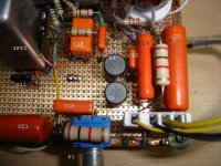
Filtering out the RF signal is made in a similar way of those inductor input rectifiers, but at the cathode of a follower, then at lower impedances, I can use sane values of inductances and capacitors. L4, L5 and C15 forms a 3 pole
T filter, designed to a crossover frequency of about 10KHz. C14 bootstraps the grid circuit of the follower, and thanks to it, more than 4MΩ is viewed from the grid, so a small AC load to the detector circuit is offered, also improving audio recovered quality. The two 36mH coils are extracted from wasted cassette recorders. A 2KΩ potentiometer in the cathode circuit is the DC and AC cathode load and also acts as a volume control, and sound take off. The triode cathode follower is one section of an ECC82 envelope. An additional advantage is that audio output is made at low impedance.
The AGC section also includes ideas from other sources. A tap in the primary of the second IF transformer is coupled to a third tuned coil, in which normal rectification is done, thanks to one of the diodes inside the EABC80 triple diode-triode tube. The amount of signal transferred from one circuit to other is dependent of the value of capacitor C11 linking them, this way the AGC signal level can be adjusted independently of the audio one.
The DC from the AM signal recovered is filtered at the higher FI frequency by C19, but audio signals are still present in the load resistor R20, whose other end returns to a fixed voltage of -2.5V provided by a (provisional) NiCd battery, also performing other tasks in the circuit. Then, the minimum bias at the AGC line is -2.5V, sufficient to the tubes selected, whose cathodes are earthed directly.
Audio signals in the load resistor are removed in the next filter section that includes a double time constant circuit R19-C17 and R18-C18 (See the behavior of this network in the simulation below). The purpose of it is to let the AGC line some gain at frequencies between 1 and 10Hz, just that may occur when rocking the dial between strong and weak adjacent station’s signal; or fading. The 100KΩ and the 3.3µF mesh doesn't account for those quick variations, giving fast response to sudden variations of incoming signals. When the tuned station signal is stable, very low frequencies are filter out by this network as ordinarily. The voltage developed at the AGC line is directly feed to the IF and converter stages by means of a low time constant decoupling networks to the bottom of the grid coils (R1-C1, R3-C5, R6-C9). Relatively high capacitor values at these points ensure easy RF return from the grid to the cathode of each tube.
RF AGC has another difference from standard circuits. Minimum negative bias is injected to the grid of the RF amplifier, via the isolated diode in V4, also contained in the EABC80 envelope. But at its anode, also is added a positive current derived from the screen grid stabilized voltage, and whose value is selected via a preset, P3 and the 10MΩ resistor R21. Diode clamps this voltage at this point to the -2.5V level. When signal strength is sufficiently strong, then the negative current flowing trough R17 from the ACG voltage developed, overcomes the positive current, and then bias to the RF stage is correspondingly increased, as D4 goes cutoff (Plate goes negative respect to its cathode). This way, RF amplification is held at a maximum for lower signal levels, making better the signal/noise ratio of the stage. This idea is called "sinking diode" borrowed from the LS book, at page 1117, figure 27.38B and the explaining text at page 1108, and adapted to my circuit. This sketch also have been used in tube TV sets, I saw some schematics using this topology.
The triode inside the EABC80, the second one in the ECC82, the full voltage of the NiCd battery and the associated circuitry performs an adjustable and stabilized 105V supply to be used by the oscillator’s plate and the screen grids of the RF amplifiers, via a decoupling resistor and capacitor in each one of them. This way the voltage is kept stable at +105V and independent of the AGC and line voltage, improving AGC action.
Plates are powered from a +275V source, via a 1KΩ resistor R12, which limits current in case of a short circuit or overload when manipulating the board (still under development), and putting across it a voltmeter, the current drawn in milliamperes is easily read. C21 decouples this bus to ground. Similar resistor is inserted in the anode of the voltage regulator (R13), for the same reasons and C22 keeps this wire to earth potential for RF signal. Decoupling between stages is made by 2.5mH coils from PC monitors and .22µF caps to the earth bus.
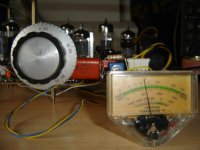
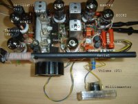
A 1mA FS 42Ω permanent-magnet moving-coil milliammeter is used as signal strength meter (S-meter), and a VTVM is constructed around a second ECC82 V6 tube. The –11.5V via a zero pot is injected to one of the triodes, while the full AGC is feed to the other. The difference between them is converted to a current who deflects the needle of this instrument. It has been designed by me to ensure full scale with about -10V at the AGC bus, sufficient for receive a local powerful station without overloading the meter.
The full spread sheet is available upon request, in Spanish and in a txt
CP437 format, made with the edit.com from MS-DOS 7.10, this file also includes some ideas (some of them not tested or implemented yet), calculus, formulas, and sundry data collected from books, the Internet and from my own imagination.
This tuner has been designed having in mind this idea, and an animus or spirit of to experiment some own ideas that I previously had in mind, and never before tested (by me) in a real circuit. Also, I used in it, materials recovered from the box of old stuff, most of them has been kept unused for more than a decade.
The first thing that I wanted to test, is an AM receiver with a RF amplifier stage, using a remote cutoff pentode, with the ferrite rod antenna (aerial) directly wired to the signal grid. Looking into my stock of tubes, I found an EF89 for the stage.
The gang condenser (G in the schematic) is triple equal sections made with brass sheets, at both stator and rotor plates, rescued from any Philips radio receiver.
The antenna (L1), the RF inter stage transformer and the oscillator coil has been designed following what is suggested in the Langford-Smith’s (LS) "Radiotron" book. The antenna I used is a rod saved from a discarded transistor radio, but rewind completely for this purpose using Litz wire, the last recovered from the inductor in wasted electronic ballast for fluorescent lamps. As I lack of characteristics or data sheets of the ferrites employed, a test coil has been made in each of them, and tested with a RLC digital meter.
RF transformer (L2) and oscillator coils (L3) use the same wire, but for them, I recycled the bobbin, the core and the magnetic shield from PC monitor horizontal width coil control.
The choused converter tube is an ECH81, the signal grid of the hexode is tied to the RF tuned transformer, and the injection grid wired together with the oscillator, which has the form of a tuned-grid tickler-coil (or Armstrong) oscillator, with series feed in both windings.
The RF and antenna coils have been calculated as is suggested in chapter 23 of the LS's book. Oscillator coil, padder and trimmers make use of the formulae at chapters 24 and 25, mainly from Section 3 of the last, in which the tracking between RF and oscillator method is described.
IF section follows those described in Chapter 26, but making use of standard double-tuned mutual-inductance-coupled transformers. The tube selected is a remote cutoff pentode type EBF89, which also includes a dual diode intended for the audio detection.
At the detector stage, start to flow my own ideas. First, the AGC line isn't derived simply filtering out the audio signal at the detector, in fact it has its own transformer (IFT3), rectifier and filter. More over, the filter isn't classic at all.
Audio signal is detected using both diodes, connected in a non standard manner. The AM signal is rectified, and no capacitors are found in the signal path to ground, because it generates audio distortion as is demonstrated by LS, and by S. Seely in his book entitled "Electron-Tube Circuits" (Pages 351 and the followings). The second diode cooperates to the signal detection, improving the rectification, acting as a shunt diode (Idea taken from the Seely's book, page 125, figure 7.4 and associated text). This way I gain more than 6dB of recovered audio respect to single diode detection with no extra components added.
Filtering out the RF signal is made in a similar way of those inductor input rectifiers, but at the cathode of a follower, then at lower impedances, I can use sane values of inductances and capacitors. L4, L5 and C15 forms a 3 pole
T filter, designed to a crossover frequency of about 10KHz. C14 bootstraps the grid circuit of the follower, and thanks to it, more than 4MΩ is viewed from the grid, so a small AC load to the detector circuit is offered, also improving audio recovered quality. The two 36mH coils are extracted from wasted cassette recorders. A 2KΩ potentiometer in the cathode circuit is the DC and AC cathode load and also acts as a volume control, and sound take off. The triode cathode follower is one section of an ECC82 envelope. An additional advantage is that audio output is made at low impedance.
The AGC section also includes ideas from other sources. A tap in the primary of the second IF transformer is coupled to a third tuned coil, in which normal rectification is done, thanks to one of the diodes inside the EABC80 triple diode-triode tube. The amount of signal transferred from one circuit to other is dependent of the value of capacitor C11 linking them, this way the AGC signal level can be adjusted independently of the audio one.
The DC from the AM signal recovered is filtered at the higher FI frequency by C19, but audio signals are still present in the load resistor R20, whose other end returns to a fixed voltage of -2.5V provided by a (provisional) NiCd battery, also performing other tasks in the circuit. Then, the minimum bias at the AGC line is -2.5V, sufficient to the tubes selected, whose cathodes are earthed directly.
Audio signals in the load resistor are removed in the next filter section that includes a double time constant circuit R19-C17 and R18-C18 (See the behavior of this network in the simulation below). The purpose of it is to let the AGC line some gain at frequencies between 1 and 10Hz, just that may occur when rocking the dial between strong and weak adjacent station’s signal; or fading. The 100KΩ and the 3.3µF mesh doesn't account for those quick variations, giving fast response to sudden variations of incoming signals. When the tuned station signal is stable, very low frequencies are filter out by this network as ordinarily. The voltage developed at the AGC line is directly feed to the IF and converter stages by means of a low time constant decoupling networks to the bottom of the grid coils (R1-C1, R3-C5, R6-C9). Relatively high capacitor values at these points ensure easy RF return from the grid to the cathode of each tube.
RF AGC has another difference from standard circuits. Minimum negative bias is injected to the grid of the RF amplifier, via the isolated diode in V4, also contained in the EABC80 envelope. But at its anode, also is added a positive current derived from the screen grid stabilized voltage, and whose value is selected via a preset, P3 and the 10MΩ resistor R21. Diode clamps this voltage at this point to the -2.5V level. When signal strength is sufficiently strong, then the negative current flowing trough R17 from the ACG voltage developed, overcomes the positive current, and then bias to the RF stage is correspondingly increased, as D4 goes cutoff (Plate goes negative respect to its cathode). This way, RF amplification is held at a maximum for lower signal levels, making better the signal/noise ratio of the stage. This idea is called "sinking diode" borrowed from the LS book, at page 1117, figure 27.38B and the explaining text at page 1108, and adapted to my circuit. This sketch also have been used in tube TV sets, I saw some schematics using this topology.
The triode inside the EABC80, the second one in the ECC82, the full voltage of the NiCd battery and the associated circuitry performs an adjustable and stabilized 105V supply to be used by the oscillator’s plate and the screen grids of the RF amplifiers, via a decoupling resistor and capacitor in each one of them. This way the voltage is kept stable at +105V and independent of the AGC and line voltage, improving AGC action.
Plates are powered from a +275V source, via a 1KΩ resistor R12, which limits current in case of a short circuit or overload when manipulating the board (still under development), and putting across it a voltmeter, the current drawn in milliamperes is easily read. C21 decouples this bus to ground. Similar resistor is inserted in the anode of the voltage regulator (R13), for the same reasons and C22 keeps this wire to earth potential for RF signal. Decoupling between stages is made by 2.5mH coils from PC monitors and .22µF caps to the earth bus.
A 1mA FS 42Ω permanent-magnet moving-coil milliammeter is used as signal strength meter (S-meter), and a VTVM is constructed around a second ECC82 V6 tube. The –11.5V via a zero pot is injected to one of the triodes, while the full AGC is feed to the other. The difference between them is converted to a current who deflects the needle of this instrument. It has been designed by me to ensure full scale with about -10V at the AGC bus, sufficient for receive a local powerful station without overloading the meter.
The full spread sheet is available upon request, in Spanish and in a txt
CP437 format, made with the edit.com from MS-DOS 7.10, this file also includes some ideas (some of them not tested or implemented yet), calculus, formulas, and sundry data collected from books, the Internet and from my own imagination.
Attachments
Very neat Osvaldo! This is quite a serious attempt at a great AM receiver design..
Did you wind the coils, and can you provide some building guidance for someone like me who might be interested in building one at some point?
Pictures?
Did you wind the coils, and can you provide some building guidance for someone like me who might be interested in building one at some point?
Pictures?
Thanks, Kevin, but it will be a large thread, but I can't find how to place an image between text lines. In other pages using this soft, appears a "place inline" button, but I could't find it here.
I think you can use "Wrap image tags around selected text" I recommend putting them in your personal gallery and linking from there.
I'm not convinced. I think only one diode (pin 7 on EBF89) actually does anything; the pin 8 diode will never see a positive voltage and turn on because the other end of the secondary of IFT2 has nothing to work against.Osvaldo de Banfield said:Audio signal is detected using both diodes, connected in a non standard manner.
Unfortunately I have the second edition of Seeley's book so I can't find the references you give. I can't find any two-diode AM detectors in the book.
I would have used a gas discharge tube for stabilising the anode voltages.
Unfortunately I have the second edition of Seeley's book so I can't find the references
you give. I can't find any two-diode AM detectors in the book.
This is an interesting article on AM demodulation.
http://tonnesoftware.com/appnotes/demodulator/EnvelopeDemodulators.pdf
Hi,
The simple fact is FM stereo is vastly superior to AM.
You can make AM better but your chasing your tail.
Comparatively AM will never get near FM.
Any attempt at "hifi" AM seems to me pointless.
Though FWIW many old tuners has good AM sections.
rgds, sreten.
The simple fact is FM stereo is vastly superior to AM.
You can make AM better but your chasing your tail.
Comparatively AM will never get near FM.
Any attempt at "hifi" AM seems to me pointless.
Though FWIW many old tuners has good AM sections.
rgds, sreten.
Thanks. I don't think I have seen that note before, although I think I saw something similar perhaps by a different author.rayma said:This is an interesting article on AM demodulation.
http://tonnesoftware.com/appnotes/de...modulators.pdf
I think only one diode (pin 7 on EBF89) actually does anything;
Yes, it does a great job. Wait a bit that the thread is still under construction.
Be patient, friends!
Hi,
The simple fact is FM stereo is vastly superior to AM.
This may be true in countries of the first world, here there exists FM stations occupying half of channel, and half of the adjacent, say, between two legal stations.
If the signal is good, I could try that AM and FM are comparable quality, the most of the problem are the poor quality of the AM receivers.
There was a time when AM provided quite acceptable quality in the UK. Obviously not as good as FM, but pleasant to listen to.
There was a time when AM provided quite acceptable quality in the UK. Obviously not as good as FM, but pleasant to listen to.
To my elderly ears AM has better intelligibility for spoken word broadcasts. Yes to FM for music but give me AM for speech.
Often the purported benefits of FM are soundly squashed by the broadcast studio equipment and practices used. Commercial broadcasters mostly employ the lowest standards allowable in order to maximise revenue.
FM's benefits are not "purported" but real: capture effect, less noise, less distortion. I agree that modern broadcast practice is to throw away these benefits in favour of a loud signal.
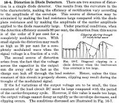
This section describes an improvement I did in the detector circuit, mainly from an own idea. It seems like a circuit that appears in a the Langford-Smith´s book in the lasts pages, but he also uses a capacitor input filter following the detector stage. But as in some books I read I found that the capacitor in an usual pi filter consisting in a series resistor of about 50K, and two capacitors of about 100pF causes increased audio distortion mainly at high modulation index and at higher audio frequencies, I had the idea to filter out (integrate) the RF signal post detector stage using a LC filter in place of the classic CRC network, as in the figure.
About this classic arrangement, it is said in the Seely´s book entitled ”Vacuum-Tube Circuits”, in chapter 16, page 351:
In the other hand, on is to use a detector circuit that has no capacitor at the input of the filter, and at high AC and DC loading, where there is also an important advantage of not to have the AGC circuit loading the detector.
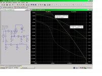
As the loading in the detector stage must be maintained high for still better audio quality at the detector and in order to reduce the loading in the FI anode circuit, the filter must be of the inductor-input type. But here, another problem arises: the inductance needed at this minute currents and high voltages, makes the inductor itself of insane values and extremely difficult to get in real world. And although such an inductor would be obtainable, it will have such high parasitic capacitances that become impossible to keep the original idea. Also capacitors in the filter network, would assume so small values, that the stray capacitors alone are much bigger than the needed for an effective filtering.
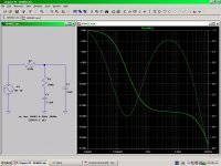
To overcome these difficulties, I decided to use the V6 triode (ECC82) as a cathode follower, and in its cathode, I put the filter as the load. This way, the inductor used is an “off the shelf” one, in fact, it has been recycled from discarded cassette recorders. They can clearly been saw in the photos above, marked as L4 and L5, and have a mark in the top that says 363 (then, 36mH). So, as I have several of them, I designed the filter to use these inductors, and I compute the overall circuit to meet the goal. Then P1 is the cathode load and its value is 2K. And as the T circuit needs the same impedance at both extremes (symmetrical), the bias of the triode has been estimated to have also about 2000 in its cathode lead. The result, is the behavior seen in the following simulation, and as a comparison, the standard CRC network is also simulated, where you can see clearly the well definite cutoff frequency, at about 10KHz, also helping to improve the overall selectivity of the entire tuner. The 500K resistors at both paths are to take into account for the reflected impedance from the anode of the IF amplifier, and the internal of the tuned circuits itself, or a part of it.

Once the signal appears detected but unfiltered in the cathode, it is positively feedforward to the bottom grid leak, for the purpose of bootstraping the grid circuit. This bootstrapping is incomplete. As the cathode follower is operating into an impedance equal to its own internal output impedance, then signal gain is only about 0.5. Then, only half the grid signal appears at its cathode, then the 2.2M resistance is only doubled, and the AC load resistance viewed from the detector is about 4.5M. But, if a still higher impedance would be used at this node, it becomes problematic any small stray capacitance, turning useless my idea. Then, the AC load for the detector is the parallel of this 4.5M and the 1M resistor R8, which is the DC loading for the diode. The coupling capacitors from the diode load to triode’s grid and from cathode to bottom side of the grid leak resistor are bypasses at both, audio and RF frequencies.
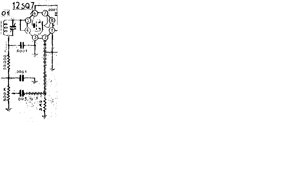
Also, a curious detector can be seen in my circuit. Both internal diodes in the EBF89 aren’t paralleled as usual, in contrast they operate out of phase, helping together to the detection of the audio signal. Consider the following circuit, also taken from the Seely’s book chapter 7, at page 125:
If you imaginary rotates the series diode though the input of the above (a) schematic, you will found its cathode together to the second diode, and then they may have the common cathode as in the EBF89 and the vast majority of the double diode triode tubes.
I find that this simple modification, which neither require any added component, enhances the audio recovery at about twice respect to the single diode configuration.
About this classic arrangement, it is said in the Seely´s book entitled ”Vacuum-Tube Circuits”, in chapter 16, page 351:
An externally hosted image should be here but it was not working when we last tested it.
In the other hand, on is to use a detector circuit that has no capacitor at the input of the filter, and at high AC and DC loading, where there is also an important advantage of not to have the AGC circuit loading the detector.
As the loading in the detector stage must be maintained high for still better audio quality at the detector and in order to reduce the loading in the FI anode circuit, the filter must be of the inductor-input type. But here, another problem arises: the inductance needed at this minute currents and high voltages, makes the inductor itself of insane values and extremely difficult to get in real world. And although such an inductor would be obtainable, it will have such high parasitic capacitances that become impossible to keep the original idea. Also capacitors in the filter network, would assume so small values, that the stray capacitors alone are much bigger than the needed for an effective filtering.
To overcome these difficulties, I decided to use the V6 triode (ECC82) as a cathode follower, and in its cathode, I put the filter as the load. This way, the inductor used is an “off the shelf” one, in fact, it has been recycled from discarded cassette recorders. They can clearly been saw in the photos above, marked as L4 and L5, and have a mark in the top that says 363 (then, 36mH). So, as I have several of them, I designed the filter to use these inductors, and I compute the overall circuit to meet the goal. Then P1 is the cathode load and its value is 2K. And as the T circuit needs the same impedance at both extremes (symmetrical), the bias of the triode has been estimated to have also about 2000 in its cathode lead. The result, is the behavior seen in the following simulation, and as a comparison, the standard CRC network is also simulated, where you can see clearly the well definite cutoff frequency, at about 10KHz, also helping to improve the overall selectivity of the entire tuner. The 500K resistors at both paths are to take into account for the reflected impedance from the anode of the IF amplifier, and the internal of the tuned circuits itself, or a part of it.
Once the signal appears detected but unfiltered in the cathode, it is positively feedforward to the bottom grid leak, for the purpose of bootstraping the grid circuit. This bootstrapping is incomplete. As the cathode follower is operating into an impedance equal to its own internal output impedance, then signal gain is only about 0.5. Then, only half the grid signal appears at its cathode, then the 2.2M resistance is only doubled, and the AC load resistance viewed from the detector is about 4.5M. But, if a still higher impedance would be used at this node, it becomes problematic any small stray capacitance, turning useless my idea. Then, the AC load for the detector is the parallel of this 4.5M and the 1M resistor R8, which is the DC loading for the diode. The coupling capacitors from the diode load to triode’s grid and from cathode to bottom side of the grid leak resistor are bypasses at both, audio and RF frequencies.
Also, a curious detector can be seen in my circuit. Both internal diodes in the EBF89 aren’t paralleled as usual, in contrast they operate out of phase, helping together to the detection of the audio signal. Consider the following circuit, also taken from the Seely’s book chapter 7, at page 125:
If you imaginary rotates the series diode though the input of the above (a) schematic, you will found its cathode together to the second diode, and then they may have the common cathode as in the EBF89 and the vast majority of the double diode triode tubes.
I find that this simple modification, which neither require any added component, enhances the audio recovery at about twice respect to the single diode configuration.
Attachments
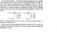
For improved performance of the AGC subsystem, I wanted to design a simple voltage regulator to give stabilized bias to the screen grid of all amplification stages; and to the oscillator, for better frequency stability. The target voltage is about +105V, because I reserved 5V for an independent resistor at each screen, with the double purpose that these resistors (together with a bypass condenser) may serve as decoupling between the different stages, and to have an easy way to measure the current drawn by each one of them.
The improvement arises from the fact that as the voltage at the control grid of a pentode (Whose screen and/or plate voltages are feed trough a dropping resistor) is raised in the negative direction to decrease the gain, the cathode current decreases, then increasing the anode and screen voltages, tending to increase the transconductance of the tube, just with the opposite tendency that we want he do. As the screen voltage mainly controls the transconductance of a pentode, stabilizing it against such voltage counteracting, the AGC needs less effort to accommodate the signal level in the tuner stages.
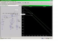
The circuit employed is very easy to understand. The triode section in the EABC80, which is of the high type, acts as a grounded cathode voltage amplifier, and in certain form like the “see-saw” circuit. In other words, like an anode follower feeding a cathode follower, in this case, is one section of the ECC82 tube, which has sufficient margin to carry the about of 8mA drawn by the amplifier, converter and oscillator stages. The anode load of the amplification tube is wired to the cathode of the regulating (series) unit, then it is bootstrapped and it is seen as a bigger resistance than its ohmic value. From a (temporarily connected) NiCd battery (9 cells for a total of about 11.5V full charged), and the grid near ground potential, it amplifies this voltage and reverses its polarity in direct proportion to the anode to grid and the grid to reference resistors. In the simulation below, the trimpot for fine adjustment of the final voltage has been omitted for clarity of the circuit.
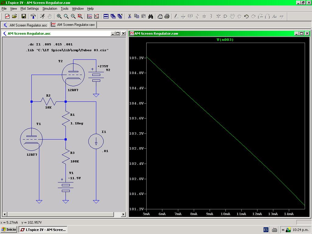
Here you can see that wide variations (about a total of 10mA, from 5mA with full AGC bias to 15mA with only the 2.5V bias base), the voltage at the screen bus is maintained within a range of 4V. Also, in the real circuit I could see that such a current variation is exaggerated, taking into account that the current drawn by the oscillator is a very stable load for this bus, in all the tuning range.
The improvement arises from the fact that as the voltage at the control grid of a pentode (Whose screen and/or plate voltages are feed trough a dropping resistor) is raised in the negative direction to decrease the gain, the cathode current decreases, then increasing the anode and screen voltages, tending to increase the transconductance of the tube, just with the opposite tendency that we want he do. As the screen voltage mainly controls the transconductance of a pentode, stabilizing it against such voltage counteracting, the AGC needs less effort to accommodate the signal level in the tuner stages.
The circuit employed is very easy to understand. The triode section in the EABC80, which is of the high type, acts as a grounded cathode voltage amplifier, and in certain form like the “see-saw” circuit. In other words, like an anode follower feeding a cathode follower, in this case, is one section of the ECC82 tube, which has sufficient margin to carry the about of 8mA drawn by the amplifier, converter and oscillator stages. The anode load of the amplification tube is wired to the cathode of the regulating (series) unit, then it is bootstrapped and it is seen as a bigger resistance than its ohmic value. From a (temporarily connected) NiCd battery (9 cells for a total of about 11.5V full charged), and the grid near ground potential, it amplifies this voltage and reverses its polarity in direct proportion to the anode to grid and the grid to reference resistors. In the simulation below, the trimpot for fine adjustment of the final voltage has been omitted for clarity of the circuit.
Here you can see that wide variations (about a total of 10mA, from 5mA with full AGC bias to 15mA with only the 2.5V bias base), the voltage at the screen bus is maintained within a range of 4V. Also, in the real circuit I could see that such a current variation is exaggerated, taking into account that the current drawn by the oscillator is a very stable load for this bus, in all the tuning range.
Attachments
This is the AGC rectifier section, and as above I said, it is independent from the audio detector.
In a tap in the plate tuned circuit of the second IF transformer (IFT2) found at about 180µH from the cold side of the coil (Which was intended originally to be used with transistors and has a 1mH permeability variable inductor and a fixed 110pF capacitor), the AM carrier and the audio envelope is taken off and applied via a small capacitor (C11 of only 3pF) to a similar tuned circuit (IFT3), but in this case it works as a single tuned circuit (autotransformer), leaving the secondary untuned and isolated from any other source of potential. Adjusting the value of this capacitor gives me a way to define the amount energy transferred from one circuit to the other, and finally, the negative DC voltage that will be applied to the amplifier’s grids. This fact can be viewed in a LT Spice simulation at the image below. Observe also, a slight detuning while varying C19’s value, which can be compensated with a counter adjust of the core in the coil. Please note that C19 makes reference to the entire schematic, renamed C3 at the schematic at left in the simulation image.
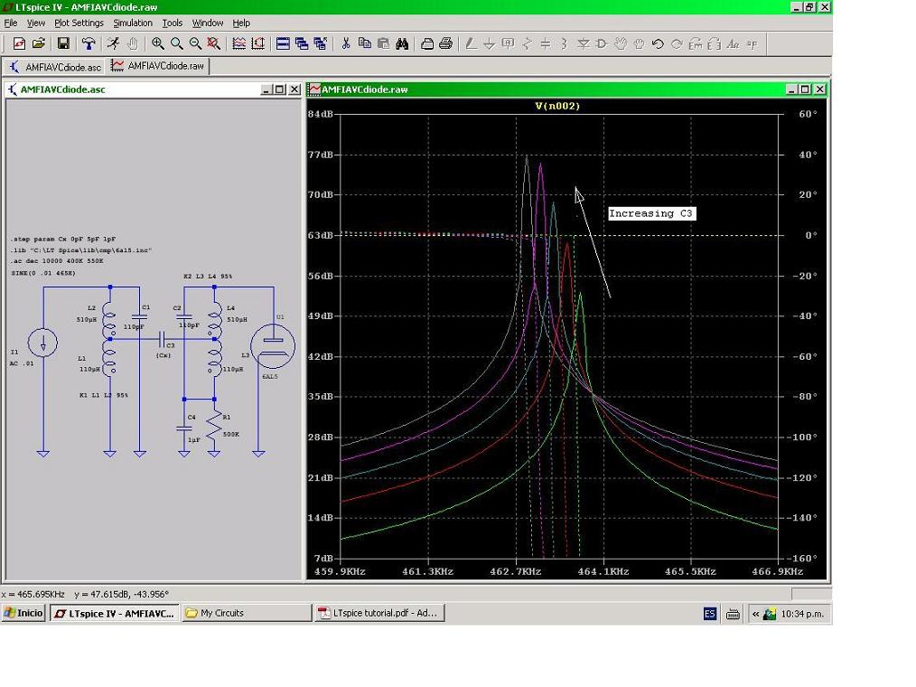
The signal appearing at the tap of IFT3, is then multiplied by the turns ratio and the Q of the circuit, which is deliberately decreased by the use of a low value of resistance load (R17, R18, R19 and R20 combined), who also returns to a source of –2.5V, actually, a tap in a NiCd battery pack. This way, there is always a minimum of –2.5V plus the contact potentials as AGC voltage, because the RF, converter and IF tube’s cathodes are grounded (earthed) directly. The signal appearing at the hot side of the tuned circuit is then rectified, and resistively added to this floor voltage. The Q of this circuit is kept low, to avoid an unpleasant effect that occurs while tuning the dial: as the AGC voltage increases when tuned to the center of the incoming signal, and decreasing to both sides, decreasing the gain, and then the volume of audio signal recovered; when the signal is just centered in the IF passband.
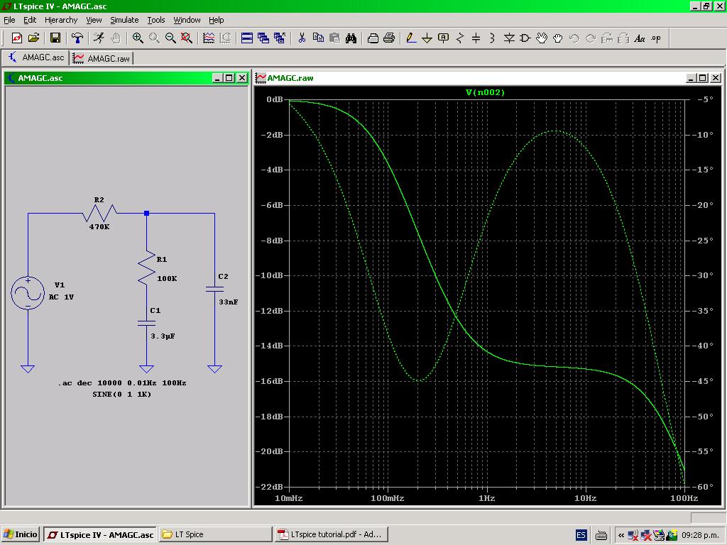
The rectified signal by diode V3 inside the EABC80 appears at the bottom, of the coil, across C19 and consists of an audio signal which has lost the RF by the action of C19, who has a low reactance to the 465KHz signal. But the audio signal at this point has appreciable amplitude, mainly the lower frequencies, because C19 (4.7nF) has an appreciable reactance to them. Then, this variable DC voltage is passed through a special low pass filter consisting of C17, C18, R18 and R19.
As can be seen in the following simulation, this networks acts in a different manner as the standard single high value series resistor and shunt capacitor, which has a constant slope of -6dB/dec. In the other hand, this (my) filter has some gain (which can be seen mainly as the FI gain [dB] plus the loss in this mesh [dB] in a closed loop negative feedback system, is bigger than zero) for a range of frequencies between 1 and 10Hz, where it has a gain plateau. It can be analyzed readily thinking that at a DC component, this network has unity gain (at no DC load). As frequency is increased from 0 Hz, the susceptance of C18 (it has a value one hundred times C19), will increase, raising the transmission attenuation through the action of R18. This happens, until its reactance equals R18. At these frequencies, C19 still has a low susceptance, and then it is kept out of action. Then, the lower terminal of R18 is effectively at ground potential, and the transfer ratio becomes R18/(R18 + R19). As we continue increasing frequency, slowly the reactance of C19 becomes more and more small shunting R18, C18 and R19 to earth, starting the final -6dB/dec slope to infinite attenuation.
The objective is that the association of the gain in the FI stage and the losses in this net, shows a net gain more than one, then being capable of compensate in a better manner, the effects of fading, to compensate the signal variations under QSV (although the receiver isn’t conceived for DX), and while rocking the dial between adjacent stations with different signal strengths levels of incoming signals.
It can be also shown in the simulation, that appreciable phase variations happens in the filter, but given the very restricted band width of the closed loop, this effect is of negligible importance.
The voltage so obtained is then, as usual, applied at the bottom side of the ferrite antenna coil, the grid winding of the RF transformer and the IF secondary winding, via a decoupling RC network, whose time constant is negligible compared with the ones of the filter above mentioned. The bypass condensers have an important value, because they must have a very low reactance at the working frequencies, and thus, they don’t affect the tracking between RF and oscillator sections. Note that C1 and C2 are effectively in series to ground in the signal path with the ganged tuning condenser.
But there is still another improvement in the AGC bus. Looking at the schematic, you can see that the negative bias obtained at the output of such filter is feed directly to the converter (Hexode section of the ECH81 tube) and the FI amplifier (Pentode inside the EBF89 bulb). But the RF amplifier (EF89) receives this voltage, by a different path. Note that the diode D2 of EABC80 has its cathode returned to the –2.5V fixed bias, but the plate receives the AGC voltage added to a positive one through a 10M resistor (R21), R22 and preset P3. In the Langford Smith’s book “Radiotron” it is called “sinking diode” scheme, but it has been also used in some early tube TV receivers. As long as the AGC voltage developed by the rectifier is low, the potential at the anode of the diode is positive to its cathode, and then the diode conducts clamping the AGC bias for the RF amplifier at said –2.5V. But if the signal received increases in amplitude, then the rectified negative signal overcomes the positive one, diode goes to cutoff and the negative grid bias for RF stage is increased from this floor. This way, the RF gain is maintained at a maximum while receiving weak signals, keeping signal to noise ratio, at a good level. As soon as the signal tuned is of sufficient magnitude to develop a high negative voltage at the AGC rectifier, then just there, starts to decrease the receiver sensitivity, when signal to noise ratio is naturally high. As an example, with the adjusted level of P3, when the signal generates a bias of –6V, then starts to overcome the positive current through R21, and for a bias of -8V, RF is about –4V. Then, The AGC mechanism is enhanced breaking the action between the RF and the converter plus the FI sections. Also, decreasing the gain of the RF amplifier at a good signal level, reduces the distortion in the FI stage, preventing its overloading. This fact can also be viewed clearly in the following simulation.
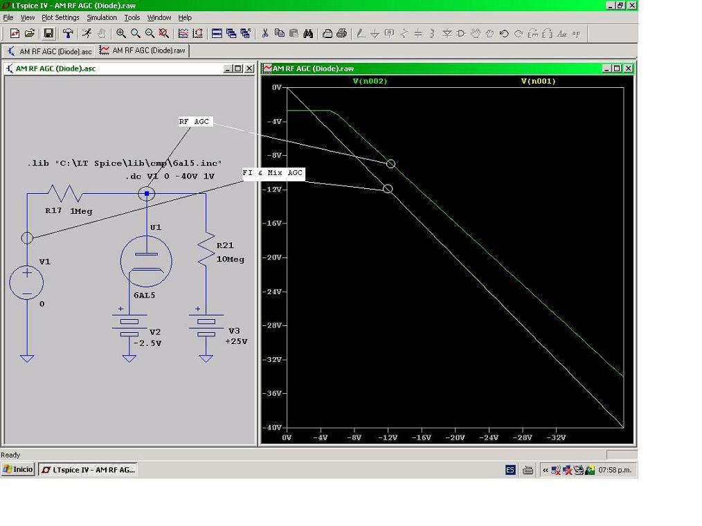
In a tap in the plate tuned circuit of the second IF transformer (IFT2) found at about 180µH from the cold side of the coil (Which was intended originally to be used with transistors and has a 1mH permeability variable inductor and a fixed 110pF capacitor), the AM carrier and the audio envelope is taken off and applied via a small capacitor (C11 of only 3pF) to a similar tuned circuit (IFT3), but in this case it works as a single tuned circuit (autotransformer), leaving the secondary untuned and isolated from any other source of potential. Adjusting the value of this capacitor gives me a way to define the amount energy transferred from one circuit to the other, and finally, the negative DC voltage that will be applied to the amplifier’s grids. This fact can be viewed in a LT Spice simulation at the image below. Observe also, a slight detuning while varying C19’s value, which can be compensated with a counter adjust of the core in the coil. Please note that C19 makes reference to the entire schematic, renamed C3 at the schematic at left in the simulation image.
The signal appearing at the tap of IFT3, is then multiplied by the turns ratio and the Q of the circuit, which is deliberately decreased by the use of a low value of resistance load (R17, R18, R19 and R20 combined), who also returns to a source of –2.5V, actually, a tap in a NiCd battery pack. This way, there is always a minimum of –2.5V plus the contact potentials as AGC voltage, because the RF, converter and IF tube’s cathodes are grounded (earthed) directly. The signal appearing at the hot side of the tuned circuit is then rectified, and resistively added to this floor voltage. The Q of this circuit is kept low, to avoid an unpleasant effect that occurs while tuning the dial: as the AGC voltage increases when tuned to the center of the incoming signal, and decreasing to both sides, decreasing the gain, and then the volume of audio signal recovered; when the signal is just centered in the IF passband.
The rectified signal by diode V3 inside the EABC80 appears at the bottom, of the coil, across C19 and consists of an audio signal which has lost the RF by the action of C19, who has a low reactance to the 465KHz signal. But the audio signal at this point has appreciable amplitude, mainly the lower frequencies, because C19 (4.7nF) has an appreciable reactance to them. Then, this variable DC voltage is passed through a special low pass filter consisting of C17, C18, R18 and R19.
As can be seen in the following simulation, this networks acts in a different manner as the standard single high value series resistor and shunt capacitor, which has a constant slope of -6dB/dec. In the other hand, this (my) filter has some gain (which can be seen mainly as the FI gain [dB] plus the loss in this mesh [dB] in a closed loop negative feedback system, is bigger than zero) for a range of frequencies between 1 and 10Hz, where it has a gain plateau. It can be analyzed readily thinking that at a DC component, this network has unity gain (at no DC load). As frequency is increased from 0 Hz, the susceptance of C18 (it has a value one hundred times C19), will increase, raising the transmission attenuation through the action of R18. This happens, until its reactance equals R18. At these frequencies, C19 still has a low susceptance, and then it is kept out of action. Then, the lower terminal of R18 is effectively at ground potential, and the transfer ratio becomes R18/(R18 + R19). As we continue increasing frequency, slowly the reactance of C19 becomes more and more small shunting R18, C18 and R19 to earth, starting the final -6dB/dec slope to infinite attenuation.
The objective is that the association of the gain in the FI stage and the losses in this net, shows a net gain more than one, then being capable of compensate in a better manner, the effects of fading, to compensate the signal variations under QSV (although the receiver isn’t conceived for DX), and while rocking the dial between adjacent stations with different signal strengths levels of incoming signals.
It can be also shown in the simulation, that appreciable phase variations happens in the filter, but given the very restricted band width of the closed loop, this effect is of negligible importance.
The voltage so obtained is then, as usual, applied at the bottom side of the ferrite antenna coil, the grid winding of the RF transformer and the IF secondary winding, via a decoupling RC network, whose time constant is negligible compared with the ones of the filter above mentioned. The bypass condensers have an important value, because they must have a very low reactance at the working frequencies, and thus, they don’t affect the tracking between RF and oscillator sections. Note that C1 and C2 are effectively in series to ground in the signal path with the ganged tuning condenser.
But there is still another improvement in the AGC bus. Looking at the schematic, you can see that the negative bias obtained at the output of such filter is feed directly to the converter (Hexode section of the ECH81 tube) and the FI amplifier (Pentode inside the EBF89 bulb). But the RF amplifier (EF89) receives this voltage, by a different path. Note that the diode D2 of EABC80 has its cathode returned to the –2.5V fixed bias, but the plate receives the AGC voltage added to a positive one through a 10M resistor (R21), R22 and preset P3. In the Langford Smith’s book “Radiotron” it is called “sinking diode” scheme, but it has been also used in some early tube TV receivers. As long as the AGC voltage developed by the rectifier is low, the potential at the anode of the diode is positive to its cathode, and then the diode conducts clamping the AGC bias for the RF amplifier at said –2.5V. But if the signal received increases in amplitude, then the rectified negative signal overcomes the positive one, diode goes to cutoff and the negative grid bias for RF stage is increased from this floor. This way, the RF gain is maintained at a maximum while receiving weak signals, keeping signal to noise ratio, at a good level. As soon as the signal tuned is of sufficient magnitude to develop a high negative voltage at the AGC rectifier, then just there, starts to decrease the receiver sensitivity, when signal to noise ratio is naturally high. As an example, with the adjusted level of P3, when the signal generates a bias of –6V, then starts to overcome the positive current through R21, and for a bias of -8V, RF is about –4V. Then, The AGC mechanism is enhanced breaking the action between the RF and the converter plus the FI sections. Also, decreasing the gain of the RF amplifier at a good signal level, reduces the distortion in the FI stage, preventing its overloading. This fact can also be viewed clearly in the following simulation.
Attachments
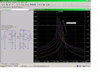
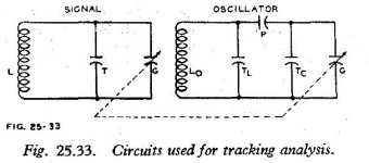
This paragraph, I transcribe a part of the calculation of the LC components for the oscillator and incoming signals of the receiver, originally made in a txt file.
To meet the objective, I used the formulae at the LS book, chapter 25, page 1005 and following. Once I had the values for my gang, whose capacitance is from 12 to 500pF measured with a digital RLC tester, I loaded the value of this components in those formulas and found the fixed capacitance, inductance, padder and trimmers needed for right tracking between oscillator and RF. Band limits were assumed to be 500 and 1650 KHz, and the crossover points coincide with this limits, plus one sited at 809KHz (root mean between the two limits).

The resulting values were:
Po = 552pF (82pF + 470pF or 220pF + 330pF) (Padder);
Tco = 14.5pF (Fixed capacitance plus about 10pF of assumed strays)
TLo = 48.4pF (Trimmer)
L3o = 84.74µH (Inductance)
for the oscillator section, and:
T1 = 27.34pF (Trimmer, plus 12pF min. Cap. of the gang, plus 10pF for strays).
L1 = 188.5µH
From the above computation, let it be Co the total capacity of the oscillator section of the gang:
Co = TLo + Po series with G3 = TLo + ((Po * (G3 + Tco)/( Po + G3 + Tco))
And let also be Cs the tuning capacity of the signal circuit:
Cs = G1 + T1 = G1 + 37.34pF
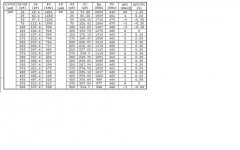
With these values, I can make a table to see how well is the tracking. Here is a first approximation:

As the results weren’t too satisfactory, mainly in the high extreme, I made a simple program in QBASIC no more than 15 lines of sentences, then I run it to verify if I can get better approach at both limits. This program gave me the following final results:
P (Padder).......................... 552 pF;
Tc (Capacity // to the Gang)........ 16 pF;
Tl (Capacity // to the inductor).... 38.4 pF;
Lo (Inductance of the oscillator)... 89 µH.
The optimized results live in the following table:

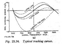
Where it can be seen the better tracking in general in all the AM band
and the reduced error which can be easily absorbed by the Q of RF tuned circuits. A slight mistracking in the very high end would be corrected adjusting the slotted end plates of the gang, but in practice, I didn’t need to do that.

To meet the objective, I used the formulae at the LS book, chapter 25, page 1005 and following. Once I had the values for my gang, whose capacitance is from 12 to 500pF measured with a digital RLC tester, I loaded the value of this components in those formulas and found the fixed capacitance, inductance, padder and trimmers needed for right tracking between oscillator and RF. Band limits were assumed to be 500 and 1650 KHz, and the crossover points coincide with this limits, plus one sited at 809KHz (root mean between the two limits).
The resulting values were:
Po = 552pF (82pF + 470pF or 220pF + 330pF) (Padder);
Tco = 14.5pF (Fixed capacitance plus about 10pF of assumed strays)
TLo = 48.4pF (Trimmer)
L3o = 84.74µH (Inductance)
for the oscillator section, and:
T1 = 27.34pF (Trimmer, plus 12pF min. Cap. of the gang, plus 10pF for strays).
L1 = 188.5µH
From the above computation, let it be Co the total capacity of the oscillator section of the gang:
Co = TLo + Po series with G3 = TLo + ((Po * (G3 + Tco)/( Po + G3 + Tco))
And let also be Cs the tuning capacity of the signal circuit:
Cs = G1 + T1 = G1 + 37.34pF
With these values, I can make a table to see how well is the tracking. Here is a first approximation:
As the results weren’t too satisfactory, mainly in the high extreme, I made a simple program in QBASIC no more than 15 lines of sentences, then I run it to verify if I can get better approach at both limits. This program gave me the following final results:
P (Padder).......................... 552 pF;
Tc (Capacity // to the Gang)........ 16 pF;
Tl (Capacity // to the inductor).... 38.4 pF;
Lo (Inductance of the oscillator)... 89 µH.
The optimized results live in the following table:
Where it can be seen the better tracking in general in all the AM band
and the reduced error which can be easily absorbed by the Q of RF tuned circuits. A slight mistracking in the very high end would be corrected adjusting the slotted end plates of the gang, but in practice, I didn’t need to do that.
Attachments

Last edited:
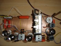
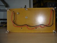
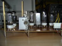
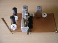
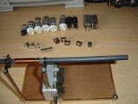
Some photos of the project, still under development.
Attachments
-
 AM Receiver Project 10.JPG154 KB · Views: 220
 -
 AM Receiver Project 09.JPG137.1 KB · Views: 201
 -
 AM Receiver Project 08.JPG141.8 KB · Views: 181
 -
 AM Receiver Project 07.JPG137.8 KB · Views: 171
 -
 AM Receiver Project 06.JPG131.2 KB · Views: 167
 -
 AM Receiver Project 05.JPG153.8 KB · Views: 179
 -
 AM Receiver Project 04.JPG127.2 KB · Views: 154
 -
 AM Receiver Project 03.JPG144.1 KB · Views: 163
 -
 AM Receiver Project 02.JPG151.1 KB · Views: 181
 -
 AM Receiver Project 01.JPG157.1 KB · Views: 191
Still more images.
Attachments

In this post I want to add some miscellanies about the project.
For those interested in repeat my line of thinking, this is an easy and simple program made for MS DOS QBASIC, which helped me to obtain a better values for the circuit elements of the oscillator and RF stages, but I suppose than can also be adapted to another programming language, surely more modern that this.
Here is the code used:
/code:
CLS
LET Tc = 16 { Value in Farad of the trimmer capacitor }
LET P = 552 { Value in Farad of the padder capacitor }
LET Tl = 38.4 { Value in Farad of the fixed capacitance in the oscillator coil }
LET Lo = .000089 { Value in Henry of the oscillator inductor }
LET Fi = 465000 { Value in Hertz of the intermediate frequency amplifier }
LET Ls = .0001885 { Value in Henry of the antenna and RF tuned inductor }
LET Ct = 37.4 { Value in Farad of the antenna trimmer capacitor plus fixed and starys }
PRINT "Fsint", "Cosc", "Fosc", "FI conv.", "Error"
FOR i = 1 TO 21
READ G { Step Gang capacitance read from data statements }
LET Cs = Ct + G { Total capacity in the RF section: gang (Read from data statements), trimmer and stray }
LET Fs = 1 / (6.28 * SQR(Ls * (Cs * 1E-12))) { Incoming signal frequency }
LET Co = Tl + (((Tc + G) * P) / (Tc + G + P)) { Total capacity in the oscillator section, gang (Read from data statements), trimmer and stray }
LET Fo = 1 / (6.28 * SQR(Lo * (Co * 1E-12))) { Oscillating frequency }
LET Fic = Fo – Fs { Intermediate frequency obtained }
LET DFi = Fi – Fic { Intermediate frequency error respect to the wanted }
PRINT Fs, Co, Fo, Fic, DFi
NEXT i
DATA 12,25,50,75,100,125,150,175,200,225,250
DATA 275,300,325,350,375,400,425,450,475,500
/end code.
The first sentence clears the screen between tests. Then, in the following, I load the fixed values of some constants that will not be changed in the program. Following it, a simple titles for the columns of results from the computations below them.
A for – next loop for the total points of the gang capacity for which is wanted to estimate the tracking error. The capacity values to be read are stored in the data sentences at the end of the program. With this value, simple frequency calculations are made for oscillator and incoming signal paths, and checked (substracted) to obtain the final error.
Bibliography:
F. Langford Smith “Radio Designer’s Handbook”, 1997.
George E. Valley and Henry Wallman “Vacuum Tube Amplifiers”, 1948.
Samuel Seely “Electron-Tube Circuits” 1950.
ARRL “Radio Amateur’s Handbook”, 1949 (Version in Spanish).
Héctor Algarra y Alberto Rodríguez “La Técnica del Receptor de Televisión” (In Spanish).
Some patents in PDF format at Google Patents, Advanced Search.
Tubes data sheets found in the Internet from Google Search.
Software:
MS DOS 7.10 edit.com
Microcap IV (For DOS) (Simulation program for DOS’ers)
Microsoft Word, Office 97
LT Spice (From http://ltspice.linear.com/software/LTspiceIV.exe)
Microsoft Paint.
Express PCB and Schematic capture at http://www.expresspcb.com
Adobe Acrobat Reader from Adobe: Creative, marketing and document management solutions
Thanks to Luciano Alvarez LW1EL for support my large comments and crazy ideas almost every Sunday nights at the QAP frequency.
- Home
- Source & Line
- Analogue Source
- High (Audio) Quality AM Tuner