...Maybe someone can point out some opamps with useful internal connections...
The AD797? Not because I am a "fanboy", as JCX would say, but there seems a clear trend to eliminate connections on modern amps.
The mass market wants simplicity and that trumps flexibility it seems.
I feel some sympathy for the simple approach after a look at the compensation of the Tek 505 and the AP SYS1 - not simple or easy to understand.
The 505 uses different compensation on each integrator and a third approach on the inverter.
The SYS1 uses yet another approach on the integrators and no obvious compensation on the inverter.
I am not that interested in the details of the 5534 compensation as such, but curious about reasons for the differences.
One integrator in the 505 is two-pole compensated and the other is not, odd.
The two-pole is referenced to earth.
Both integrators on the SYS1 are two-pole and bootstrapped, kind of like Edmond Stuart's TMC from my initial look, and referenced to +15V.
Presumably the reference to +15V is for improved PSRR.
Anyone have any ideas how all this plays out in the AD797?
Best wishes
David
Last edited:
There is also the MAX9632 but the current noise...
Yes, about twice the current noise and not balanced by better performance in other areas, except convenience features like lower power consumption.
So, not a contender for my use.
Best wishes
David
...[505] two-pole is referenced to earth.
the SYS1 are two-pole and bootstrapped, kind of like Edmond Stuart's TMC from my initial look, and referenced to +15V.
Presumably the reference to +15V is for improved PSRR.
Anyone have any ideas how all this plays out in the AD797?
Kind of surprised no one has commented on this, with Samuel's and David[a]'s expertise in the 505 and Sys1, the similarity to Edmond's TMC, Scott's tie to the 797, Demian's question, and the issue of PSRR in amps with no actual earth connection that is a special subject of JCX.
Must have been I didn't state my questions well.
Where should the two-pole compensation be referenced?
The 505 uses earth, the Sys1 uses +15V while JCX's simulations use -15V.
I can simulate this but want to understand the principles.
Harry Dymond looked at this for an amp with an earth but how does it work in an op-amp?
JCX has several times posted a link that sets limits on PSRR as function of other op-amp specifications, but it provides no actual recommendations.
Does the TMC-like output connection of the Sys1 alter the analysis?
Best wishes
David
Last edited:
Scott's tie to the 797,
Best wishes
David
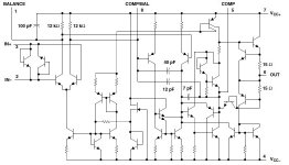
There is at least one missing aspect, it was not unknown to split the comp cap on op-amps and reference 1/2 to Vcc and 1/2 to Vee also there is a substrate parasitic. Frankly I can not remember where the plates and the substrate parasitics were tied on the 797. These facts could lead to some folklore around different op-amps and bypassing/layout configurations.
Hi Scott,
You really don't want to start the Hi Fi industry talking about that, do you?
I grant you that it could be extremely amusing.
-Chris
You really don't want to start the Hi Fi industry talking about that, do you?
I grant you that it could be extremely amusing.
-Chris
Hi Dave,
I think there is more to the SYS1 scheme than just compensation.
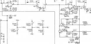
What does the 100 ohm resistor do tied to pins 6 and 5. Will this increase the bias current in the output stage or is it boot strap?
The comp is not tied to +15v it tied to +15v1. This is a n RC filtered/regulated point.
Anything directly in the signal path is tied to this point including the mdacs. The Mdacs don't have a PSSR. They have a power supply sensitivity usually given in percent and require separate down regulation.
I think it's done this way to avoid the PSSR issues with tying the compensation to one of the rails.
I think there is more to the SYS1 scheme than just compensation.
What does the 100 ohm resistor do tied to pins 6 and 5. Will this increase the bias current in the output stage or is it boot strap?
The comp is not tied to +15v it tied to +15v1. This is a n RC filtered/regulated point.
Anything directly in the signal path is tied to this point including the mdacs. The Mdacs don't have a PSSR. They have a power supply sensitivity usually given in percent and require separate down regulation.
I think it's done this way to avoid the PSSR issues with tying the compensation to one of the rails.
Attachments
Last edited:
What does the 100 ohm resistor do tied to pins 6 and 5...?
I hoped you would tell me😉
My first impression is that it's a bootstrap but I didn't look closely, don't want to waste time if it is specific to the 5534.
Hopefully someone will tell us both, or else I will have to think.
The comp is not tied to +15v it tied to +15v1. This is a n RC filtered
Well spotted, I did notice that but didn't think much about it so I didn't mention it.
Intuitively makes sense to tie to a quiet point, maybe +15v1 is just convenient.
I think it's done this way to avoid the PSSR issues with tying the compensation to one of the rails.
Self and Harry Dymond have some useful comments about this in a power-amp context that assumes an earth reference is available.
I will have to reread them and think unless JCX already has the answer from his earlier device level simulation of the 797.
Best wishes
David
Where should the two-pole compensation be referenced?
Generally speaking where the emitter (of the CE stage that is compensated) is referenced to. This ensures that both ends of the capacitor that connects to the input stage are referenced to the same potential at low frequencies. Thus supply ripple doesn't cause a current flow to the second stage.
What does the 100 Ohm resistor do tied to pins 6 and 5. Will this increase the bias current in the output stage?
Yes, that's a class A biasing technique.
Samuel
...where the emitter (of the CE stage that is compensated) is referenced to. This ensures that both ends of the capacitor that connects to the input...
Well, the 797 only has one section and no Miller capacitor so it's a bit different to the usual.
But now I look at the simplified schematic it seems clear that it should be the minus supply.
...it was not unknown to split the comp cap on op-amps and reference 1/2 to Vcc and 1/2 to Vee also there is a substrate parasitic. Frankly I can not remember where the plates and the substrate parasitics were tied on the 797...
Don't say that just when I think I have the answer.😉
The simplified schematic in the datasheet shows a connection to the minus supply, not sure I want my simple faith to be disturbed.
Best wishes
David
Yes, that's a class A biasing technique.
Samuel
Quite a bit too, looks like 5-6mA?
Quite a bit too, looks like 5-6mA?
I may miss something here, but why is this technique called "class A biasing"?
It appears to me the purpose of this technique is to displace the bias point of half of the output stage, so that the total large signal transconductance is less peaking around the crossover, leading to less large signal gm doubling distortions.
Granted, one could get a similar effect by truly biasing the output stage (both halves) towards class A, but increasing the bias current of half of the output stage is not "class A" and may have several important negative side effects (like asymmetrical output stage input impedance, displacing the chip isotherms, etc...)
Well, the 797 only has one section and no Miller capacitor so it's a bit different to the usual.
How would you like to apply two-pole compensation to the AD797 when its compensation capacitor is internal? There might be a clever arrangement with the distortion cancellation/decompensation pin.
Likely the residual distortion of the AD797 is dominated by effects which a modified compensation scheme would not reduce (voltage-dependent loading of the compensation node). Also ~100 MHz GBW is plenty for a 100 kHz oscillator (regarding Q enhancement).
Samuel
I may miss something here, but why is this technique called "class A biasing"?
It appears to me the purpose of this technique is to displace the bias point of half of the output stage, so that the total large signal transconductance is less peaking around the crossover, leading to less large signal gm doubling distortions.
Granted, one could get a similar effect by truly biasing the output stage (both halves) towards class A, but increasing the bias current of half of the output stage is not "class A" and may have several important negative side effects (like asymmetrical output stage input impedance, displacing the chip isotherms, etc...)
If you look at the circuit it is an all npn output stage, pull-down is through a diode to the output and the npn on the bottom. The resistor increases the current through the whole chain. Notice the diode connected npn is connected on the side of the 15 Ohm resistor that senses the output current (short circuit limit).
EDIT - It might be fun to stick a pnp like a 2N4258 there as an experiment (base to comp pin, emitter to output, and collector to -V), but it will probably sing.
Edit - The 5534 is analysed at length in Dr. Huijsing's book https://books.google.com/books?id=W...IHDAA#v=onepage&q=5534 all npn output&f=false
Last edited:
I may miss something here, but why is this technique called "class A biasing"?
It appears to me the purpose of this technique is to displace the bias point of half of the output stage, so that the total large signal transconductance is less peaking around the crossover, leading to less large signal gm doubling distortions.
Granted, one could get a similar effect by truly biasing the output stage (both halves) towards class A, but increasing the bias current of half of the output stage is not "class A" and may have several important negative side effects (like asymmetrical output stage input impedance, displacing the chip isotherms, etc...)
These are good observations, and many of us are a bit sloppy with our semantics for convenience, including me. If it is just pulling current down from the top NPN transistor of the output stage, then it is pretty much equivalent to the technique that many use with ordinary op amps to force them into "class A" operation over a limited output current range by connecting a resistor (or current source) to the negative rail. This indeed displaces the crossover point.
Related to this, Doug Self patented this technique for use in audio power amplifier output stages and dubbed it "crossover displacement" (XD) and uses it in some commercial amplifiers, I believe. The novelty, if there is any, is that he controls the value of the pull down current source dynamically in accordance with the output voltage. This works to some extent for fixed resistive loads, but not really for reactive loads or loads of significantly different impedance from which the XD circuit is optimized. I think he pulls about an amp. This means that the bottom PNP output transistor runs cold most of the time. It is also a little bit unclear how he sets the bias at the displaced crossover to satisfy the Oliver criteria. The XD circuit is described in his book.
Anyway, the technique as described for op amps can probably be said to create a single-ended class A region over a limited output current range.
Cheers,
Bob
I played with ad797 compensation with my simplified transistor level model - not very sophisticated but does show some features
http://www.diyaudio.com/forums/solid-state/123613-class-biasing-ad797-6.html#post1525757
the 2nd shows a "T", 2-pole compensation attempt with the 797 "error correction" output C divider and the R to the negative rail
the example is for ~30 dB gain, which I think is a bit higher than SVO gains
http://www.diyaudio.com/forums/solid-state/123613-class-biasing-ad797-6.html#post1525757
the 2nd shows a "T", 2-pole compensation attempt with the 797 "error correction" output C divider and the R to the negative rail
the example is for ~30 dB gain, which I think is a bit higher than SVO gains
The 2nd shows a "T", 2-pole compensation attempt with the 797 "error correction" output C divider and the R to the negative rail
the example is for ~30 dB gain, which I think is a bit higher than SVO gains.
Thanks!
Samuel
This means that the bottom PNP output transistor runs cold most of the time
The 5534 has no pnp, the resistor increases both pull up and pull down transistor quiescent current.
The 5534 has no pnp, the resistor increases both pull up and pull down transistor quiescent current.
I quickly checked the schematic, you are correct, but then the 5534 output stage doesn't appear to be a regular Class AB either, not even quasi-comp.
I was thinking more about the standard complementary output stage that the rail resistor unbalances.
The 5534 has no pnp, the resistor increases both pull up and pull down transistor quiescent current.
Hi Scott,
I was referring to the crossover displacement audio power amplifier output stage.
I realize that at the time of the 5534 there were no decent vertical PNP transistors in junction-isolated linear IC processes, and we had to live with the old lateral PNPs. Once I got to design with verticals I never looked back 🙂.
Cheers,
Bob
- Home
- Design & Build
- Equipment & Tools
- Low-distortion Audio-range Oscillator