Acko, could you please describe what connector is the I2C and the pin-out? Add to the manual?
//
//
Oops I read the post from TNT wrong. He has the miniStreamer, I used the USBStreamer, so the pin outs are wrong.
John, do the USBStreamer accept 32b data?
Did you run the Acko ADC as shipped?
//
OK, I have the board mounted - thats why I missed it. Thanks!
Something was linked as I took away a bridge that was there when delivered.
What kind of behavior shall I expect if set to SW but not SW setting has been performed?
//
OK, so I have mixed up the strapping. Forget about HW/SW. It was one of the pads for setting fs that I had desoldered 🙁
//
Sofware Mode
Software control of the ADC gives more flexibility for different arrangements. This is done by
the I2C port that is connected to the header J11. An external I2C controller can then issue
commands to set the ADC registers. The ADC module is supplied with factory default settings
for Hardware mode only. To enable software mode please note the following:
1. Locate solder pads marked 'C' and 'D'. They have solder pad links and factory
default hardware mode set with ‘0’ link for ‘D’ and ‘1’ link for ‘C’
2. Enable pull-ups. Remove the '0' link from 'D' and then bridge the '1' link
instead. No change for ‘C’ if it is already linked to ‘1’. Note: if external I2C
device has pull-ups already then remove all links on ‘C’ and ‘D’.
3. The I2C address is set default to ADRR Pin=1 (0x96). If you wish to use ADDR Pin=0 (0x94) then link pads marked
"ADR0” (underneath the board)
4.[Optional] link the pads marked “SW” underneath the board.
This will now enable I2C comms to the ADC Module. Also, I2C is 3.3V type and make sure your external controller is a 3.3V system. For more information on I2C control of registers refer to the ES9102 datasheet.
Please note that custom Digital RIAA Filters or Biquad filter programming are not supported in this module.
I2C interface J11 pin assignment:
Pin#1 – Clip Interrupt output (active high default). Option for open collector via register setting and “E” pad link to ‘1’ (remove link ‘0’ first)
Pin#2 – SCL
Pin#3 – SDA
Pin#4 – GND
....
What kind of behavior shall I expect if set to SW but not SW setting has been performed?
//
Register defaults in SW mode are listed in the 9102 Datasheet
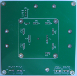
Can you by the aid of these pictures give me a hint on how to connect this? I'm a bit confused around the C and D straps - they seem to control the fs in HW mode. Do they have other function is SW mode? Please explain.
Attachments
Can you by the aid of these pictures give me a hint on how to connect this? I'm a bit confused around the C and D straps - they seem to control the fs in HW mode. Do they have other function is SW mode? Please explain.
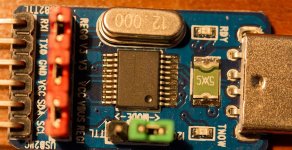
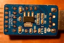
I have already explained the C and D strap connection in the previous post. In SW mode these become I2C points - see Schema for details.
Your I2C module looks compatible for direct connection. I am assuming from the pics there are no pull-ups on this module so you need to ensure ADC module has pull-ups enabled, again refer to previous post.
Thanks - sorry I think it is clear now!
If I wanted to buy a connector / cable to mate with the on board I2C connector -what shall I search for?
//
If I wanted to buy a connector / cable to mate with the on board I2C connector -what shall I search for?
//
Last edited:
If I wanted to buy a connector / cable to mate with the on board I2C connector -what shall I search for?
//
Mating connector:
Molex PN: 0510210400 available from Digikey PN:WM1722-ND or Farnell PN:9733116
Cables (pre-crimped, click fit) 150mm Molex PN: 0006660012, Digikey PN:WM2319-ND, Farnell PN: 1125272
Last edited:
Do the ADC use 7 or 8 bit addressing on I2C?
//
As per I2C standard: 7bits for chip address and 1bit for R/W.
Hey Acko,
I follow your comments on using software mode via my MCU if I decide to go that route. It looks like I can just buy one and experiment with getting it working as john has done in hardware mode. I have to build a power amp first though. I was planning on building a diy flat phono stage in front of the ADC, any suggestions ? Also can I connect it SE or do I have to configure the ADC for that first? Probably the manual goes over this 🙂
I follow your comments on using software mode via my MCU if I decide to go that route. It looks like I can just buy one and experiment with getting it working as john has done in hardware mode. I have to build a power amp first though. I was planning on building a diy flat phono stage in front of the ADC, any suggestions ? Also can I connect it SE or do I have to configure the ADC for that first? Probably the manual goes over this 🙂
TNT,
I use an Arduino. The device address is 0x4B. Acko used the device address when the pin is pulled high. (The BIII pin is low so it uses 0x40.)
No problem getting reading and writing to it.
I sent you a PM.
John
I use an Arduino. The device address is 0x4B. Acko used the device address when the pin is pulled high. (The BIII pin is low so it uses 0x40.)
No problem getting reading and writing to it.
I sent you a PM.
John
Many thanks John. Your post and PM clears a few think up for me so that I can progress my project.
//
//
Hey Acko,
I follow your comments on using software mode via my MCU if I decide to go that route. It looks like I can just buy one and experiment with getting it working as john has done in hardware mode. I have to build a power amp first though. I was planning on building a diy flat phono stage in front of the ADC, any suggestions ? Also can I connect it SE or do I have to configure the ADC for that first? Probably the manual goes over this 🙂
Yes, you can control the ADC with an external MCU but you will need to program it to match. Input can be SE or differential but the drive from your phono/preamp stage needs to be configured accordingly. Manual has some suggestions for input drive to ADC.
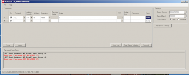
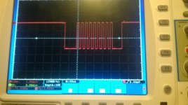
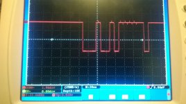
Thanks again for the answer. May I steal som more time from you please... I do see things happening on the SCL and SDA lines as I hit enter in my terminal application but I get read error code.
I'm puzzled how to use the input fields. The field "Data" seem to indicate how many bytes the read operation shall do. Can you see any obvious faults in the settings? SDA and SCL scope shots using one-shot trigger.
Thanks for any help here 🙂
//
I'm puzzled how to use the input fields. The field "Data" seem to indicate how many bytes the read operation shall do. Can you see any obvious faults in the settings? SDA and SCL scope shots using one-shot trigger.
Thanks for any help here 🙂
//
TNT,
I use an Arduino. The device address is 0x4B. Acko used the device address when the pin is pulled high. (The BIII pin is low so it uses 0x40.)
No problem getting reading and writing to it.
I sent you a PM.
John
Attachments
Thanks Acko,
I will look at the manual when I get to that point. Got a few other projects first. I will try to use it at first without any programing if possible, similar to others. Is there a manual download somewhere? Also, I was able to google and find registry settings for the sabre32 dacs. not sure there are any sites out in the web where any of the ADC registers are posted. It's hard to get access to the proper docs for these sabre chips. 🙁
I will look at the manual when I get to that point. Got a few other projects first. I will try to use it at first without any programing if possible, similar to others. Is there a manual download somewhere? Also, I was able to google and find registry settings for the sabre32 dacs. not sure there are any sites out in the web where any of the ADC registers are posted. It's hard to get access to the proper docs for these sabre chips. 🙁
Thanks Acko,
I will look at the manual when I get to that point. Got a few other projects first. I will try to use it at first without any programing if possible, similar to others. Is there a manual download somewhere? Also, I was able to google and find registry settings for the sabre32 dacs. not sure there are any sites out in the web where any of the ADC registers are posted. It's hard to get access to the proper docs for these sabre chips. 🙁
PM me with your email and I will arrange a copy of the manual (for the module only). Chip manual not permitted to be posted on a public domain, sorry.
Just to let you all know again that the ES9102 ADC chip has been discontinued and I am now down to the last few pieces. No plans at this stage for alternative design for DIYers as there is simply not enough volume to justify development.
Last edited:
- Status
- Not open for further replies.
- Home
- Source & Line
- Digital Line Level
- ADC using ES9102/9112