Ok
I am back on track.
I have done some measurements today. Maybe not 100% correctly but it gives some picture (or not?).
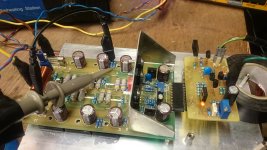
I have plugged all stuff as build and than I have removed the R13,R14 and R22 resistors (predrivers base stoppers and fancy Vbe resitor), and I didn't spoted any diffrence.
I have also replaced 220R resistor biasing the drivers with 180R and there is a bit of the improvement --> the outputs are switching off quicker (current measurement with no load at fast square/sine waves).
The one thing spotted --> the fancy Vbe resistor R22 really works, the OP bias vs VAS bias is more stable with it. But this doesn't matter now.
But all stuff was done with Toshiba OP transistors.
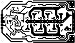
Now I am making second board for the onsemi transistors with few changes:
-more air in between the tracks
-separate ground return for decoupling caps
-separate ground return for RC networks
-less copper at the low current part of the PCB (smaller copper track area schould help here)
-added second resistor for biasing the predrivers --> so the bases of the predrivers will see less of the copper track
-added spaces for Miller caps at the drivers (just in case)
-removed base stoppers at predrivers
I really tryed to see the fire (like in Ed Sheeran's song 😛) but no joy.
I was thinking about ''fusing'' the drivers and OP transistors together but to check it out I will need the board with the problem on it.
OS
That could be the issue here.
In my previous boards like in post 658 I was powering the OP transistors and the drivers from the same spot (no RC network).
I think only Terry can check it out --> cut two collector tracks form the drivers and solder them to the OP transistors tracks.
But I am wondering why I do not have issues at my board 🙁 I will put tomorrow 0,33R resistors instead of fuses and will check --> good point.
I am back on track.
I have done some measurements today. Maybe not 100% correctly but it gives some picture (or not?).
I have plugged all stuff as build and than I have removed the R13,R14 and R22 resistors (predrivers base stoppers and fancy Vbe resitor), and I didn't spoted any diffrence.
I have also replaced 220R resistor biasing the drivers with 180R and there is a bit of the improvement --> the outputs are switching off quicker (current measurement with no load at fast square/sine waves).
The one thing spotted --> the fancy Vbe resistor R22 really works, the OP bias vs VAS bias is more stable with it. But this doesn't matter now.
But all stuff was done with Toshiba OP transistors.
Now I am making second board for the onsemi transistors with few changes:
-more air in between the tracks
-separate ground return for decoupling caps
-separate ground return for RC networks
-less copper at the low current part of the PCB (smaller copper track area schould help here)
-added second resistor for biasing the predrivers --> so the bases of the predrivers will see less of the copper track
-added spaces for Miller caps at the drivers (just in case)
-removed base stoppers at predrivers
I really tryed to see the fire (like in Ed Sheeran's song 😛) but no joy.
I was thinking about ''fusing'' the drivers and OP transistors together but to check it out I will need the board with the problem on it.
OS
That could be the issue here.
In my previous boards like in post 658 I was powering the OP transistors and the drivers from the same spot (no RC network).
I think only Terry can check it out --> cut two collector tracks form the drivers and solder them to the OP transistors tracks.
But I am wondering why I do not have issues at my board 🙁 I will put tomorrow 0,33R resistors instead of fuses and will check --> good point.
Attachments

Last edited:
Terry
You are brave man!!
I will make this board with MJL outputs anyway - I am well puzzled really.
The thing with the fuses can be easly checked --> You can throw the fuses away and putt the jumper instead.
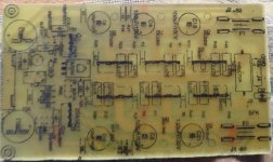
The files are bellow. I have changed the base stoppers to 10R (many amps are using 10R stoppers).
The 100pF caps at the drivers will not make any damage.
Tomorrow I will solder the resistors instead of fuses to simulate the bad connection so If you can wait till tomorrow I will know the answer for that questoin and the layout can be redone in 10s.
Edit:
In CFP-Mad IPS change the 100pF cap in the input RF filter with 330pF or 220pF if you have in stock.
2nd Edit:
Terry
I have moved second RC network behind the drivers. New files in atatchment.
Regards
You are brave man!!
I will make this board with MJL outputs anyway - I am well puzzled really.
The thing with the fuses can be easly checked --> You can throw the fuses away and putt the jumper instead.
The files are bellow. I have changed the base stoppers to 10R (many amps are using 10R stoppers).
The 100pF caps at the drivers will not make any damage.
Tomorrow I will solder the resistors instead of fuses to simulate the bad connection so If you can wait till tomorrow I will know the answer for that questoin and the layout can be redone in 10s.
Edit:
In CFP-Mad IPS change the 100pF cap in the input RF filter with 330pF or 220pF if you have in stock.
2nd Edit:
Terry
I have moved second RC network behind the drivers. New files in atatchment.
Regards
Attachments
Last edited:
Borys,
I hope you and Terry work this out, this is an interesting build with the output devices moved closer to the center-line of the board. I would like to see it with only one pair of output devices at one point. perhaps the MT-200 devices?
I hope you and Terry work this out, this is an interesting build with the output devices moved closer to the center-line of the board. I would like to see it with only one pair of output devices at one point. perhaps the MT-200 devices?
Borys,
I hope you and Terry work this out, this is an interesting build with the output devices moved closer to the center-line of the board. I would like to see it with only one pair of output devices at one point. perhaps the MT-200 devices?
We already have one of those with Latfets.
Borys, here we go again.
Attachments
That is simply not possible to do it so quick. WOW
Just in case you can cut the power supply track from driver and solder it to the OP transistor rail.
Just in case you can cut the power supply track from driver and solder it to the OP transistor rail.
Terry,
I though that single pair board was the same as the standard Slewmaster with just one pair of output devices, not a narrower version?
I though that single pair board was the same as the standard Slewmaster with just one pair of output devices, not a narrower version?
Terry,
I though that single pair board was the same as the standard Slewmaster with just one pair of output devices, not a narrower version?
Attachments
Thanks Terry,
So how is this board you are working on now different than that besides the board layout? Is that single pair enough to drive you pair of JBL speakers to a decent level?
So how is this board you are working on now different than that besides the board layout? Is that single pair enough to drive you pair of JBL speakers to a decent level?
Thanks Terry,
So how is this board you are working on now different than that besides the board layout? Is that single pair enough to drive you pair of JBL speakers to a decent level?
I built the little Latfet board before Jason narrowed it and it drives my JBL's just fine.
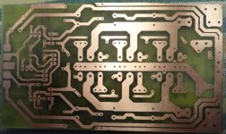
Borys' board is slightly longer and slightly narrower. The good thing is, with the three pair it can handle +-60V maybe more.
Attachments
Thank you again Terry. I'm guess just by looking at the proportions that Jason's board is about 3" x 4"? That is nice that Borys's board will take three pairs of op devices. Not much bigger in length and definitely narrower. What is the board size on Borys's boards?
Thank you again Terry. I'm guess just by looking at the proportions that Jason's board is about 3" x 4"? That is nice that Borys's board will take three pairs of op devices. Not much bigger in length and definitely narrower. What is the board size on Borys's boards?
Jason's board is 7.6cm x 10cm and Borys' board is 7cm x 12cm. Jason's was 3"x4" but I asked him to trim it down to 10cm to meet the limit for the prototype discount.
Terry,
Could you point me to the schematic for that mosfet mini OPS?? Thanks
Hi Carl,
You can find it in post #181 in the group buy thread.
Blessings, Terry
Kinderhorn,
You could put double die EXICON ECW20N20-Z/ ECW20P20-Z parts on the mosfet OPS to double the power without making a change to the PCB.
Thanks Terry
You could put double die EXICON ECW20N20-Z/ ECW20P20-Z parts on the mosfet OPS to double the power without making a change to the PCB.
Thanks Terry
Last edited:
Thank you Carl,
I'm not exactly sure how that works, is that double die parallel outputs that work in series or what? How does that work with only three legs?
I'm not exactly sure how that works, is that double die parallel outputs that work in series or what? How does that work with only three legs?
Thank you Carl,
I'm not exactly sure how that works, is that double die parallel outputs that work in series or what? How does that work with only three legs?
Looks like they are just double the power. 200V 16A for the Exicon vs 160V 7A for the Renesas.
- Home
- Amplifiers
- Solid State
- SlewMaster Builds