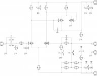
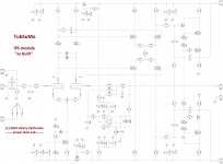
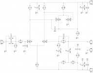
Funny way of drawing the diagram.... VAS inside the IPS. new fashion..??
Isn't it cool? 😀
Good basis for a bridged design by the way. Instead of grounding the right VAS FET's drain, the second OPS can be connected to it, plus a simple CMCL circuit for common mode stability - for those who needs more power...
Balanced, you gain power, but loose the music. 🙂
NOT cool way of drawing, as most people will have difficulty understanding the circuit. and since this is DIY, i think that we as contributes must follow the unwritten formats.
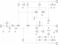
NOT cool way of drawing, as most people will have difficulty understanding the circuit. and since this is DIY, i think that we as contributes must follow the unwritten formats.
Balanced, you gain power, but loose the music. 🙂
NOT cool way of drawing, as most people will have difficulty understanding the circuit. and since this is DIY, i think that we as contributes must follow the unwritten formats.
I'm not an electronics guru by any means and I can figure out his diagrams easily enough. The software itself makes the diagrams a little tricky to follow though. Small font and thin lines are tough to follow when it's close together.
I'm not an electronics guru by any means and I can figure out his diagrams easily enough. The software itself makes the diagrams a little tricky to follow though. Small font and thin lines are tough to follow when it's close together.
And when expanded it runs out of screen. Is it possible to make it smaller but still readably?
And when expanded it runs out of screen. Is it possible to make it smaller but still readably?
I've been experimenting with the software to make it more ledgible without a lot of luck. It can be made smaller by lowering the resolution of the picture but the the lines become even thinner and harder to follow. Line width can be increased but then the whole component library would need to be redrawn to match. It's wonderful software to design with but not so much for displaying schematics.
Actually increasing the line width to .015" in the view tab helps quite a bit with viewing in the forum.
Attachments
Last edited:
I've been experimenting with the software to make it more ledgible without a lot of luck. It can be made smaller by lowering the resolution of the picture but the the lines become even thinner and harder to follow. Line width can be increased but then the whole component library would need to be redrawn to match. It's wonderful software to design with but not so much for displaying schematics.
Actually increasing the line width to .015" in the view tab helps quite a bit with viewing in the forum.
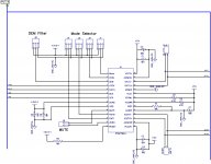
I decreased the resolution and here is the result, for me much better.
Attachments
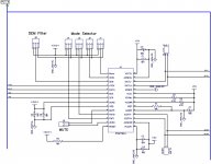
It depends on the algorithm used for decreasing the size/resolution.
The forum viewer does it in a very easy way, reducing the line thickness so that they are barely visible.
I have decreased the resolution with high quality software - looks much better.
Is it good enough (attached)?
The forum viewer does it in a very easy way, reducing the line thickness so that they are barely visible.
I have decreased the resolution with high quality software - looks much better.
Is it good enough (attached)?
Attachments
It depends on the algorithm used for decreasing the size/resolution.
The forum viewer does it in a very easy way, reducing the line thickness so that they are barely visible.
I have decreased the resolution with high quality software - looks much better.
Is it good enough (attached)?
It's much better. It's simple to increase your line thickness in Diptrace too. View/line width. That makes printed copies easier to read at the same time.
It depends on the algorithm used for decreasing the size/resolution.
The forum viewer does it in a very easy way, reducing the line thickness so that they are barely visible.
I have decreased the resolution with high quality software - looks much better.
Is it good enough (attached)?
I use Painting to change resolution.
Hi Guys
Very interesting designs, Vzaichenko!
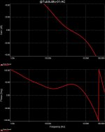
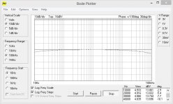
The closed-loop phase plot in post-116 looks worrisome. The steep phase reversal above the -3dB looks like assured oscillation to me, so I always adjust the compensation until this becomes a smoother rolloff. But compensation and phase margins can be tricky...
Do you have some thoughts about that?
Have fun
Very interesting designs, Vzaichenko!
The closed-loop phase plot in post-116 looks worrisome. The steep phase reversal above the -3dB looks like assured oscillation to me, so I always adjust the compensation until this becomes a smoother rolloff. But compensation and phase margins can be tricky...
Do you have some thoughts about that?
Have fun

Hi Valery
The post-116 phase plot for closed loop has a near vertical phase reversal below 10MHz. It has been my experience that such steep changes of phase - even if quite small - can lead to oscillation. It does not seem to matter if the shifts are past the transition frequency.
Is it your view that such a phase plot is okay?
Have fun
Hi Valery
The post-116 phase plot for closed loop has a near vertical phase reversal below 10MHz. It has been my experience that such steep changes of phase - even if quite small - can lead to oscillation. It does not seem to matter if the shifts are past the transition frequency.
Is it your view that such a phase plot is okay?
Have fun
Ah, I see now what you mean. Well, I had rather similar picture with a few designs in the past (also two-pole), but it did not cause any issues as far as the gain margin is good enough. In any case, real prototype behavior is always a bit different from the simulated one - too many factors make some influence, including the layout, wiring, OPS local stability, etc. So, we'll see 🙂
Example - original TubSuMo front-end, much more complicated (simulated / measured in combination with the same Lateral FET OPS). TMC compensation, rather similar phase plot picture (although, ULGF is definitely lower). Stable, top sound quality hybrid.
However, it required certain compensation adjustment during initial live testing, comparing to the simulated values.
However, it required certain compensation adjustment during initial live testing, comparing to the simulated values.
Attachments
-
 TubSuMo-Margins.JPG77.3 KB · Views: 282
 -
 @TubSuMo-as-built-sch.jpg492.8 KB · Views: 315
 -
 21-zIMD-14-15KHz-4VRMS.JPG200.3 KB · Views: 69
 -
 21-THD-20KHz-4VRMS.JPG195.6 KB · Views: 71
 -
 21-THD-10KHz-4VRMS.JPG196 KB · Views: 73
 -
 21-THD-01KHz-4VRMS.JPG196.3 KB · Views: 136
 -
 DSC03439.JPG331.8 KB · Views: 253
 -
 zDSC03435.JPG303 KB · Views: 261
Tested!
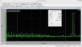
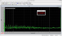
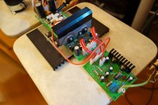
Soldered and tested one channel. With LFET OPS (TubSuMo) it ran not perfectly - local micro-oscillations in OPS were visible at high amplitude.
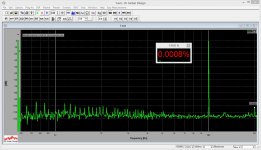
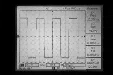
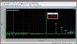
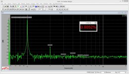
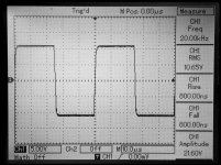
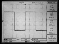
However, with IRFP-based OPS it runs very good - although I had to decrease the VAS quiescent current to 12mA (increased R4, R10, R12). Basic measurements are attached. I like the harmonics level and profile, pretty low noise, rather clean square wave response, phase response is cool for such a simple VFA topology (Bode plot).
I can't audition it now - all my speakers are moved to the other apartment now, so I will check the sound in about 2 weeks from now.
Updated gerbers are available on request - 2 resistors less now 😉
Cheers,
Valery
Soldered and tested one channel. With LFET OPS (TubSuMo) it ran not perfectly - local micro-oscillations in OPS were visible at high amplitude.
However, with IRFP-based OPS it runs very good - although I had to decrease the VAS quiescent current to 12mA (increased R4, R10, R12). Basic measurements are attached. I like the harmonics level and profile, pretty low noise, rather clean square wave response, phase response is cool for such a simple VFA topology (Bode plot).
I can't audition it now - all my speakers are moved to the other apartment now, so I will check the sound in about 2 weeks from now.
Updated gerbers are available on request - 2 resistors less now 😉
Cheers,
Valery
Attachments
-
 02-Bode-01.JPG69.1 KB · Views: 89
 -
 01-THD-20KHz.JPG206.2 KB · Views: 92
 -
 01-THD-10KHz.JPG210 KB · Views: 97
 -
 01-THD-01KHz.JPG195.7 KB · Views: 100
 -
 01-DSC03904.JPG377.8 KB · Views: 90
 -
 01-DSC03903.JPG371.9 KB · Views: 133
 -
 01-DSC03902.JPG307.7 KB · Views: 194
 -
 01-AllFET-IPS-03.jpg166 KB · Views: 176
Hi Valery,
Can this be built single sided for etching? I would like the Gerbers please.
Blessings, Terry
Can this be built single sided for etching? I would like the Gerbers please.
Blessings, Terry
Single-sided layout for etching
Hi Terry and All,
Attached is a slightly updated single-sided PCB layout for etching - traces side in pdf is mirrored.
Cheers,
Valery
Hi Terry and All,
Attached is a slightly updated single-sided PCB layout for etching - traces side in pdf is mirrored.
Cheers,
Valery
Attachments
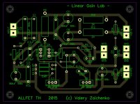
Hi Valery,
If you find time, could you please post the foil as a JPG like you did with the silk? For iron transfer I need non mirror foil and mirror silk. If you can just post the foil like you did the silk, as a jpg, that would work .
Blessings, Terry
If you find time, could you please post the foil as a JPG like you did with the silk? For iron transfer I need non mirror foil and mirror silk. If you can just post the foil like you did the silk, as a jpg, that would work .
Blessings, Terry
Last edited:
- Status
- Not open for further replies.
- Home
- Amplifiers
- Solid State
- "Compact" VFA