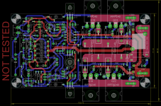
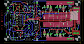
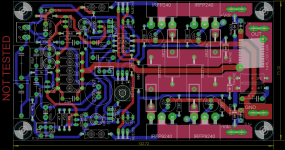
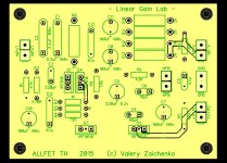
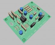
I spent a little more time for more cosmetics changes on board. These has lost 2 more mm in length but much effort has been spend to avoid layer swap on tracks
Marc
Marc
Attachments
Last edited:
I realize they are expensive, but would any of these work?I'd like to try it myself but my 2SK117s seem to be on the slow boat from China.
InterFET JFET | Mouser
2N4341 for example
I realize they are expensive, but would any of these work?
InterFET JFET | Mouser
2N4341 for example
I don't know enough about the devices to pick out a substitute myself. My 2SK117's have been on order for well over a month so they should arrive any time now.
I don't know enough about the devices to pick out a substitute myself. My 2SK117's have been on order for well over a month so they should arrive any time now.
It was not the good time to order in china beacause of "china new year celebration". Many store are on holiday.
Marc
Well to start with you compare each spec one by one.I don't know enough about the devices to pick out a substitute myself.
the 2N4341 is pretty close to 2sk117 from what I can see. I ain't no expert either, maybe others can enlighten us as too if they are close enough for this application.
I ordered them from Futurelec. Their website said they had them in stock. Three weeks later they said they were waiting for their order to arrive, while their website still said they had them in stock. Needless to say this is my last order from them.
Well to start with you compare each spec one by one.
the 2N4341 is pretty close to 2sk117 from what I can see. I ain't no expert either, maybe others can enlighten us as too if they are close enough for this application.
I was looking at the RDS. It looks pretty high to me but I don't see a spec for it from Toshiba.
Thx for the heads up on Futurelec, some things are in the "to good to be true category"
Rds, lets see if I have this correct
2sk117: Idss at 10V Vds = 1.2 - 14 mA
10/1.2mA = 8.333K ohm
10/14mA = 714 ohm
For 2n4340-4341
Drain Source ON Resistance rds(on) 1500 - 800ohm VGS = ØV, ID = Ø A f = 1 kHz
Drain Saturation Current (Pulsed) IDSS
4340 = 1.2-3.6 mA
15V/1.2mA = 12.5K ohm
15V/3.6mA = 4166 ohm
4341 = 3-9 mA for VDS = 15V, VGS = ØV
15V/3mA = 5000 ohm
15V/9mA = 1666 ohm
Seems to be less spread for the 2n4340-4341, but rds is higher for sure.
Last edited:
In overall, 2N4338-4341 is a very good low noise series of jfets.
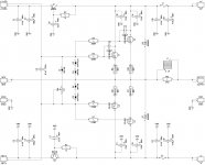
2N4338 will work here with the following adjustments (schematic from the POST#88):
R5 = 0 (jumpered);
C14 = 6.8pF
All the others from this series (4339-4341) have got too positive source potential (higher bias, especially 4341), that can be compensated by additional diode or LED in series with the source (the closer the feedback return point to zero - the better). So - possible, but requires additional testing.
So it is not Idss nor rds it is the pinch off voltage that is more important = go figure, goes to show how much I know, picked the wrong sub 🙂 thx
Well, this is a specialty of this particular "singleton" input stage arrangement 🙂
In symmetric design it wouldn't be that important...
In symmetric design it wouldn't be that important...
I built my first singleton, using a 2n4393 followed by a NE5533(dual) RIAA phono stage, it sounded pretty good.
Any idea how Semelab ALF16N16W/ALF16P16W would fair in this design? I know that the bias generator can be simplified, to passive R's, any anticipated compensation changes?
Any idea how Semelab ALF16N16W/ALF16P16W would fair in this design? I know that the bias generator can be simplified, to passive R's, any anticipated compensation changes?
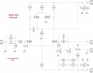
ALLFET IPS
New project in the Compact VFA series. FET-o-mania 😛
4 MOSFETs, relatively high-current operation. High linearity, low distortion, good stability margins, rather simple though. Bootstrap.
Planned for using with TubSumo Lateral FET OPS (schematic is attached for your reference). Power supply voltage +/-50V.
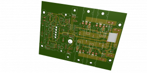
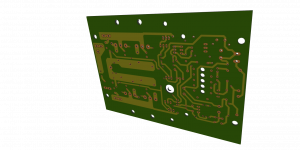
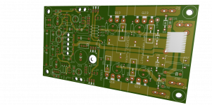
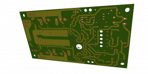
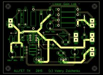
Developing a through-hole PCB for initial testing.
New project in the Compact VFA series. FET-o-mania 😛
4 MOSFETs, relatively high-current operation. High linearity, low distortion, good stability margins, rather simple though. Bootstrap.
Planned for using with TubSumo Lateral FET OPS (schematic is attached for your reference). Power supply voltage +/-50V.
Developing a through-hole PCB for initial testing.
Attachments
I am impressed, very elegant and simple. I want to build one! Please share once you have it running.
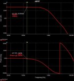
Hi Carl, yes - working on it, will let you know as soon as it's tested and measured 😉
Cheers,
Valery
Cheers,
Valery
- Status
- Not open for further replies.
- Home
- Amplifiers
- Solid State
- "Compact" VFA