corr. total
Greg Stewart x2
ppap64 x 2
Peterma x 3 V2
kenlaumm x 2 V2
j.burtt x 2
crowlie x3 V2
ed linssen x2 V2
mravinsky x2 V2
palmito x2 V2
Greg Stewart x2
ppap64 x 2
Peterma x 3 V2
kenlaumm x 2 V2
j.burtt x 2
crowlie x3 V2
ed linssen x2 V2
mravinsky x2 V2
palmito x2 V2
Attenuation update.
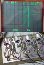
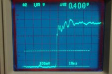
Parts arrived today and i had some spare time to do a little bit of testing.
Images attached.
- Biased at 940mV (top left of scope shot)
-Rising edge of bck/le, notice the change in speed of the waveform after 700mv. I played around with some different resistor values which got it looking a bit better than this, still have to experiment. I need to get some shorter ufl cables, i have a feeling my 100mm long cables may be degrading the signal. I think this circuit belongs on the pins of the tda.
Most importantly - It works, so thats a plus.
🙂
Feel free to comment - I know there is rather big holes in my knowledge of this stuff.
Attachments
Last edited:
*corr. total
Greg Stewart x2
ppap64 x 2 V2
Peterma x 3 V2
kenlaumm x 2 V2
j.burtt x 2
crowlie x3 V2
ed linssen x2 V2
mravinsky x2 V2
palmito x2 V2
Greg Stewart x2
ppap64 x 2 V2
Peterma x 3 V2
kenlaumm x 2 V2
j.burtt x 2
crowlie x3 V2
ed linssen x2 V2
mravinsky x2 V2
palmito x2 V2
Different values in circuit.
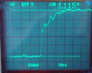
Hi Guys,
Thought this was worth sharing.
Changed a few values in the circuit and a substantial improvement in the waveform of BCK/LE.
Notice the spikes labeled D1-D4, i'm thinking these are the diodes turning on?
Oh, and C3 in the schematic was left out.
Also notice where 1.4V(1541 reference voltage) is in each example.
Attachments

Last edited:
Is R3 and C1 the input equivalent of the dac chip input pins?
Might be worth looking at different types of diodes as some of the very high freq ones have quite different characteristics, IIRC - not too sure tho ....
If you were to redesign the pcb so the output pins (instead of the ufl sockets) lined up directly above the dac chip pins and mount this new brd directly above dac chip or design it as an edge connection 'header board' next to the dac chip pins altho not sure about which 0 volt point to use, 5 or 14 ... the input ufl sockets don't necessarily have to be in line, on the edge, etc and it doesn't have to look pretty - can be 4 modules in a 'fan/radial shape', + supply and 0V bottom layer, for example...
Is R3 and C1 the input equivalent of the dac chip input pins?
Might be worth looking at different types of diodes as some of the very high freq ones have quite different characteristics, IIRC - not too sure tho ....
If you were to redesign the pcb so the output pins (instead of the ufl sockets) lined up directly above the dac chip pins and mount this new brd directly above dac chip or design it as an edge connection 'header board' next to the dac chip pins altho not sure about which 0 volt point to use, 5 or 14 ... the input ufl sockets don't necessarily have to be in line, on the edge, etc and it doesn't have to look pretty - can be 4 modules in a 'fan/radial shape', + supply and 0V bottom layer, for example...
R3 was just for experimental purposes - In the simulation it reduced overshoot.
C1 represents the 1541 input capacitance.
Ive got some "BAS16H" diodes in the same package, ill give them a go and see what happens.
Ill definitely redesign the pcb, but it will be integrated on V2.🙂
very cool. Looks great.
Hi Walter,
Thanks, its also showing some promise through the speakers too.
Greg Stewart x2
ppap64 x 2 V2
Peterma x 3 V2
kenlaumm x 2 V2
j.burtt x 2
crowlie x3 V2
ed linssen x2 V2
mravinsky x2 V2
palmito x2 V2
xaled x2 V2
ppap64 x 2 V2
Peterma x 3 V2
kenlaumm x 2 V2
j.burtt x 2
crowlie x3 V2
ed linssen x2 V2
mravinsky x2 V2
palmito x2 V2
xaled x2 V2
Melf resistors
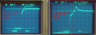
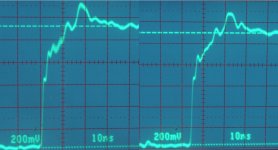
Direct comparison.
-470R MELF for R1 R2
-470R thin film for R1 R2
Diodes- bas16h
R3 0R
At the moment i'm using:
1n4148 diodes, MELF 470R(R1R2) - Keeps the reference voltage of 1.4V very close to middle of total amplitude. Waveform looks better overall - 2nd photo attached.
Direct comparison.
-470R MELF for R1 R2
-470R thin film for R1 R2
Diodes- bas16h
R3 0R
At the moment i'm using:
1n4148 diodes, MELF 470R(R1R2) - Keeps the reference voltage of 1.4V very close to middle of total amplitude. Waveform looks better overall - 2nd photo attached.
Attachments
Last edited:
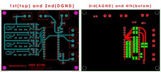
Possible v2 design
Attached is a rough draft of how the v2 design is progressing.
-4 layer PCB
-pin 5 is now isolated from digital gnd
-layer 2 and 3 are tied together at pin 14 (dgnd)
- -15v is now coupled to -5v and +5v
I'm really very pleased with how this signal attenuation circuit has turned out. Ive had a few people confirm an increase in sound quality. Must get a few more opinions, and do some blind ABX tests before I go ahead with a test pcb.
Attachments
Changed over the 4 diodes to some I had on hand - bas16h
1n4148 looks better. Just the DC bias looks a bit high.
Correction.
Descriptions in the photo should be swapped. (1n4148 has the healthier looking waveform).
Last edited:
Hi Luke,
Caps sizes are the same, dimensions had to change to make room for atten circuitry. At the moment it measures 85mm by 65mm.
Caps sizes are the same, dimensions had to change to make room for atten circuitry. At the moment it measures 85mm by 65mm.
Very nice Ryan. Wish I hadn't bought the V1 boards. Lol. Layout is much more ideal
over V1. Btw should consider regulators on the pcb as well. .
over V1. Btw should consider regulators on the pcb as well. .
Think of this as Distinction Reference Edition
I am using the classic version and no regrets. Will I upgrade to the V2? Absolutely as a 4 layer design with I2S attenuation will give that reference design edge. It will also be more expensive to fabricate, and a bunch more tiny little parts to solder.
Likely the classic (V1) is more than enough for most systems. I will likely list mine in the swap meet for anyone wanting a fast and cost effective TDA.
Great work Ryanj.
Possible suggestion
Ryanj
It would be interesting if there was an option to use larger caps on the voltage rails. No issue with the spacing for the current caps. I would like the option to use on hand Black Gates. Typically these have wider spacing on the leads. Some pcbs have 3 holes so that larger caps can be inserted or the current size. I can imagine you might prefer not to have this option to keep design clean. No worries, just a thought for consideration.
Updated list
Greg Stewart x2
ppap64 x 2 V2
Peterma x 3 V2
kenlaumm x 2 V2
j.burtt x 2
crowlie x3 V2
ed linssen x2 V2
mravinsky x2 V2
palmito x2 V2
xaled x2 V2
noizas x4 V2
Greg Stewart x2
ppap64 x 2 V2
Peterma x 3 V2
kenlaumm x 2 V2
j.burtt x 2
crowlie x3 V2
ed linssen x2 V2
mravinsky x2 V2
palmito x2 V2
xaled x2 V2
noizas x4 V2
- Status
- Not open for further replies.
- Home
- Source & Line
- Digital Line Level
- Group buy/Interest list - TDA1541A Core board.