Hi Pete,
I know we have moved way beyond this, but I wanted to try the Gnome so I built one but I can find the method for setting the trimmers. Could you please run that by me so I can get that one working?
Thanks, Terry
I know we have moved way beyond this, but I wanted to try the Gnome so I built one but I can find the method for setting the trimmers. Could you please run that by me so I can get that one working?
Thanks, Terry
For the infidel, did you try using 26mV degeneration for the IPS? Currently it is high, meaning transconductance will be halved when the IPS goes into class B, which will shift compensation frequencies. This is the same reason 26mV is used as the bias point for BJT output stages. With 26mV degeneration, idle Gm is the same as Gm at excursions. You might get better slew behavior.
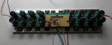
I felt Q1/Q2 and they run pretty warm but then, I didn't use the little heatsink like Thimios did. I used KSA992/C1845. I suppose I should have matched them better but it runs fine. I didn't use a socket on this one so I couldn't try it without the servo. I played it for about 4 hours and the sink on the VAS barely gets warm so it is probably not needed. I'd like to build another one and try the B option with low voltage devices but I'll probably wait until Jeff finishes his layout and have some boards made.
"I didn't use the little heatsink like Thimios did. "
This used just for thermal coupling not for cooling
Hi Pete,
I know we have moved way beyond this, but I wanted to try the Gnome so I built one but I can find the method for setting the trimmers. Could you please run that by me so I can get that one working?
Thanks, Terry
I "nuked" the gnome , all the nads , most of the infidel (still have the .asc).
Gone forever.
However , memory says the gnome had two trimmers. I usually make the 1/2
mark close to optimal. Start there (1/2). If the gnome has a servo , that's it.
If you want to adjust Ivas , adjust both trimmers to a lower resistance (higher Ivas) , reverse for lower.
Same to calculate Ivas . I (main Re) - I led = Ivas.
OS
JW and Thimios,
So now using smd devices along with all those transistors how small can you actually make this input section if that is the object?
Is there a surface mount 1 watt resistor?
I keep trying to get a handle on how small this all can really be done. Two pairs of output devices in the power section bjt or mosfet and this input all on one board and only the ouput devices full scale thru hole where need be, everything else smd.
Will you then have new problems with board layout and having to fix any problems with traces having to be moved around?
I believe that the key to the Infedel is to run it so the IPS never leaves class A, with only 26 mV over the degeneration it leaves class A and you get spikes through everything.
Looking at all the CFA's here on DIY I do find Valery's SMD mosfet VAS rather tempting. It reminds me of a circuit from an amplifier I once owned and hold in high regards.
Looking at all the CFA's here on DIY I do find Valery's SMD mosfet VAS rather tempting. It reminds me of a circuit from an amplifier I once owned and hold in high regards.
For the infidel, did you try using 26mV degeneration for the IPS? Currently it is high, meaning transconductance will be halved when the IPS goes into class B, which will shift compensation frequencies. This is the same reason 26mV is used as the bias point for BJT output stages. With 26mV degeneration, idle Gm is the same as Gm at excursions. You might get better slew behavior.
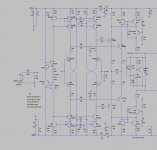
I DO have the .asc (below). I do not see where anything is not always
conducting right up to the final output devices. Where is the class B ?
Funny thing is , the attached .asc runs perfectly.
BTW , keen ... do you have a better ksa992 model ?
OS
Attachments
JW and Thimios,
So now using smd devices along with all those transistors how small can you actually make this input section if that is the object?
Is there a surface mount 1 watt resistor?
I keep trying to get a handle on how small this all can really be done. Two pairs of output devices in the power section bjt or mosfet and this input all on one board and only the ouput devices full scale thru hole where need be, everything else smd.
Will you then have new problems with board layout and having to fix any problems with traces having to be moved around?
With SMT the size of the board is set by how many traces are on it more-so than the number of components. If you don't mind a million vias you can easily go 25% size of through hole on a complex circuit. Audio circuits aren't as complex but are more critical of routing so I'm not sure how they work out. I've just finished laying out Dadod's MK2 preamp (My first audio SMT board). It came out about 2/3 the size of through hole but it's all on one side of the board. SMT components can be placed on both sides of the board but we home hackers have trouble baking pieces that way. The parts on the bottom side will fall off in the oven. In production they can hold the components in place to bake. We rely on the surface tension of the molten solder to align the parts so we can't hold parts in place.
Large current parts like 1W resistors are available but are better to use through hole devices. They emit too much heat. They will brown the PC board.
Where should C2 ground to? Should it go back directly to the star ground or go in with the servo and ground lift diodes?
Where should C2 ground to? Should it go back directly to the star ground or go in with the servo and ground lift diodes?
Nope , different than the "C". A DC coupled diamond (no caps like the VSSA) ,
would nearly go to 30VDC with just .6V of DC on the "lifted" input ground.
I do this test on all the IPS's , this design failed the test initially.
My suspicions were reinforced by Bonsai's "NX" ... same as my "correction".
Serving the diamond itself (like Vzaichenko's CFA) or the NFB node
would of also allowed a full lifted reference.
VFA's use a high Z servo return , which also is immune to this.
SO , everything individually references to G2 ...
lifted input ground is separate (with it's own return to G2).
Just observe the current layout.
OS
Sorry, no class-B here's is my take on a working infedell.
/M
Going to this 20+ device level was discussed on the first "failure".
Your design is closer to the CFA IC that inspired me. Mirroring
the current sources which are referenced to ground is what the IC
does.
I won't go for that many devices to get another 200V slew rate.
THD is about the same as the ND with 14 devices.
Build it ! man.
OS
JW,
So I assume then that when they do two layer smd boards they use fixtures to hold the components in place on the bottom layer while they are baking both the top and bottom layers? When using both sides is it that you are moving things together or that the traces can be shorter or cross over each other? I guess it is all these things combined. I guess you need to think in 3d rather than a simple 2d layout to take maximum advantage of dual layers or more.
So I assume then that when they do two layer smd boards they use fixtures to hold the components in place on the bottom layer while they are baking both the top and bottom layers? When using both sides is it that you are moving things together or that the traces can be shorter or cross over each other? I guess it is all these things combined. I guess you need to think in 3d rather than a simple 2d layout to take maximum advantage of dual layers or more.
I saw the change in the lifted ground. You've got C2 grounded with D1, D2 & R3 along with all the servo grounds.
So C2 should return to the star, D1, D2 & R3 return to the star separately and the servo return separately again? I'm trying to return the servo decoupling caps separately from the audio circuits too.
So C2 should return to the star, D1, D2 & R3 return to the star separately and the servo return separately again? I'm trying to return the servo decoupling caps separately from the audio circuits too.
JW,
So I assume then that when they do two layer smd boards they use fixtures to hold the components in place on the bottom layer while they are baking both the top and bottom layers? When using both sides is it that you are moving things together or that the traces can be shorter or cross over each other? I guess it is all these things combined. I guess you need to think in 3d rather than a simple 2d layout to take maximum advantage of dual layers or more.
I've never actually seen the baking process in production but that's how I assume they do it. I'll hand solder some larger devices on the bottom if I'm pressed for space.
The most space savings comes from being able to place one device directly over top of another. Yes think in 3D. Sometimes placing an IC diagonally can make connections a whole lot easier too. Being able to compress the layout has got to help with external interference as well. Short traces jumping from side to side on the board looks like a disaster but there's next to no parallel runs to induce noise.
O---
I'd rather build some other IPS'ss, though I could see an option with the infedel to create a balanced input.
When looking at IPS/VAS and current feedback most circuits here are good, the last one with the super pair in particular and also Valery's SMD version with mosfet VAS. Those are the two unique ones. Those concepts will in modified versions find their way to the pin-header of my OPS.
Again I would always choose the simple circuit, but spare no effort to create good non modulated housekeeping. In SMD its easy to get Doubles or Quads so complexity in housekeeping is really not a big hassle.
Attachments
OS,
If you were to build a Slewmaster with the Krypton-C or ND and you only needed 30 watts output, what single pair of output devices would you use? I'm thinking about the tweeter amp and how do you limit the output of the amp but still use the topology?
If you were to build a Slewmaster with the Krypton-C or ND and you only needed 30 watts output, what single pair of output devices would you use? I'm thinking about the tweeter amp and how do you limit the output of the amp but still use the topology?
I saw the change in the lifted ground. You've got C2 grounded with D1, D2 & R3 along with all the servo grounds.
So C2 should return to the star, D1, D2 & R3 return to the star separately and the servo return separately again? I'm trying to return the servo decoupling caps separately from the audio circuits too.
C2/R2 , the D1/2 + R3 , and any servo decoupling can all go down one trace.
This covers all the low current returns.
This trace should enter the midpoint of the G2 pad. On each side of that
pad , the relatively high current returns (current feedback and zener
decoupling) enter.
At that midpoint , opposing current pulses will cancel.
Since you are double sided , get anal and route the main rail caps returns
(C8/9) right to the G2 pad , as well. Perfect cancellation.
OS
Sounds good. That's pretty much how I've got it layed out. I'm going bug eyed from staring at it so I'll have to double check the layout later.
Last edited:
- Home
- Amplifiers
- Solid State
- Slewmaster - CFA vs. VFA "Rumble"