There is no direct equivalent for jFETs: you have the Vp, the negative voltage necessary to to block the drain current completely and the Idss, the drain current when Vg=0An fet question I've always wanted to ask and relevant here, in terms of the DC component what is the relationship of the voltage at the source and the voltage at the gate? I know that with a bjt its -0.6v and for a MOSFET -2~4 volts (Vth).
Because from the graph you can see that the low-frequency impedance is ~2.5 megohm: 1/2.5=0.4Can I trouble you to explain why it's 0.4 uA instead of 0.5 uA ?( sorry, I don't have the mu symbol on this tablet so u is used instead, you probably figured this already, but thought I should clarify for any other readers )
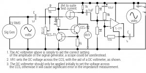
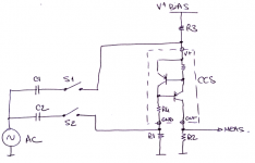
A practical test-jig could look like that (it is more advantageous to use a negative supply).
The values can be altered to suit your requirement. Here, the DC bias voltage will be variable from 2 or 3V to more than 10V and it can accommodate currents up to ~10mA (a little less if you're unlucky with the BF256B).
The Idss of the FET has to be > than the maximum test current.
There are FEts with a very large Idss, but don't use them needlessly: they will have a larger capacitance and the minimum possible test voltage will be larger too (unless you use a different supply arrangement).
During the measurement, don't leave the DC voltmeter connected, as it will skew the results.
If you wish, you can also add an opamp gain block, x10 for example, this will give you more comfort and resolution
Attachments
Siliconix jfet app notes from Archive.org JFETs Application notes
its useful to know the "triode/pentode" Vds operating regions
more on long/short channel fet and cascoding for ccs
its useful to know the "triode/pentode" Vds operating regions
more on long/short channel fet and cascoding for ccs
Last edited:
Thanks guys. I came up with my own scheme adapted from Elvees suggestions. ( see attached )
For the 2 transistor current source, the impedance is likely to be higher than the one transistor CCS, is that right?
The figure of 0.5 UA was based on my misreading of the graph, I had taken it to read 2 meg. 🙄
Do you think there is a significant advantage in using the positive ground scheme?
For the 2 transistor current source, the impedance is likely to be higher than the one transistor CCS, is that right?
The figure of 0.5 UA was based on my misreading of the graph, I had taken it to read 2 meg. 🙄
Do you think there is a significant advantage in using the positive ground scheme?
Attachments
Last edited:
The Idss of the FET has to be > than the maximum test current.
There are FEts with a very large Idss, but don't use them needlessly: they will have a larger capacitance and the minimum possible test voltage will be larger too (unless you use a different supply arrangement).
I have a variety of jfets j201, bf244a, bf245b, 2n5457, 2n5458, etc, I reckon I should be able to find one with a suitable Idss, come to think about it with test currents probably around the micro-amp region then most of them should be suitable, presumably the DC bias on the test signal would need to be adapted to different jfets?
EDIT: Ignore the last paragraph, you are talking about the DC current through the CCS, aren't you!
I have a couple of 2sk170, I think they have a larger Idss, though I'll need to confirm that.
Thanks again for everyone's help.
Last edited:
Yes (the DC/LF one at least)For the 2 transistor current source, the impedance is likely to be higher than the one transistor CCS, is that right?
Yes, it relaxes the requirements on the quality of the supply (real supplies aren't like spice voltage sources)Do you think there is a significant advantage in using the positive ground scheme?
If you test your CCS in the µA region, you have to use a FET as small as possible, BC264A or similar. A 2SK170 would be a very poor choice.I have a variety of jfets j201, bf244a, bf245b, 2n5457, 2n5458, etc, I reckon I should be able to find one with a suitable Idss, come to think about it with test currents probably around the micro-amp region then most of them should be suitable, presumably the DC bias on the test signal would need to be adapted to different jfets?
EDIT: Ignore the last paragraph, you are talking about the DC current through the CCS, aren't you!
I have a couple of 2sk170, I think they have a larger Idss, though I'll need to confirm that.
Thanks again for everyone's help.
The DC Vbias is the one you want to apply to your CCS; it won't be exactly that present on the gate because of the Vgs, which is why you need to measure the actual DC voltage. If you change the CCS current, it will change slightly
Yes, it relaxes the requirements on the quality of the supply (real supplies aren't like spice voltage sources)
Yes, I thought that might be the reasoning. What about if I were to add say an electrolytic and a 100n ceramic across the DC power rails physically close to the circuit?
If you test your CCS in the µA region, you have to use a FET as small as possible, BC264A or similar. A 2SK170 would be a very poor choice.
I was thinking about 1~10 mA test current as I would probably be using a current in this region when using the CCS as an active load for either CE or EF amplification stages, several of the jfets that I have should accommodate this range of test current.
I presume that it would be wise to test for suitable jfets in terms of their Idss, given the often 1:5 production spread.
You'll probably need more than that if you want to resolve and measure reliably sub-mV signals, but it is certainly doable.Yes, I thought that might be the reasoning. What about if I were to add say an electrolytic and a 100n ceramic across the DC power rails physically close to the circuit?
That said, why opt for a technically inferior and more difficult solution, when all you need is a little mental gymnastic to straighten the mirror-reversed image? Unless of course there is a hard reason for your choice, like the minus pole of your supply tied to the earth.
.I was thinking about 1~10 mA test current as I would probably be using a current in this region when using the CCS as an active load for either CE or EF amplification stages, several of the jfets that I have should accommodate this range of test current
Basically, try to use a FET that has an Idss just sufficient for the job: this will ensure a minimum of parasitic capacitance and lowest residual voltage
Yes, for a one-off, it is an option. Otherwise, sorted types, like BFxxx or BCxxx reduce the spread to a 1:2 ratio approximatelyI presume that it would be wise to test for suitable jfets in terms of their Idss, given the often 1:5 production spread.
Thanks again Elvee
Actually there is no good reason, so I will most likely follow your advice. I'm not sure when I'm going to be doing the actual building and testing but I will document results and share when the time comes, in the meantime I'll be doing family stuff as it is Easter break.
Gordon.
You'll probably need more than that if you want to resolve and measure reliably sub-mV signals, but it is certainly doable.
That said, why opt for a technically inferior and more difficult solution, when all you need is a little mental gymnastic to straighten the mirror-reversed image? Unless of course there is a hard reason for your choice, like the minus pole of your supply tied to the earth.
Actually there is no good reason, so I will most likely follow your advice. I'm not sure when I'm going to be doing the actual building and testing but I will document results and share when the time comes, in the meantime I'll be doing family stuff as it is Easter break.
Gordon.
CCS impedance measuring scheme latest draft
Having taken on board all suggested embellishments of my CCS impedance measuring Scheme, I now present what I hope is as close to a final draft as possible. ( see attachment )
My only concern is if the 500k input resistance of the TL071 based preamp is high enough?
I realise that with a bifet opamp there would be the opportunity to go much higher with in effect only the DC bias network resistors setting the input resistance.
Attachments
decent mA range cascode ccs will look like a C by even moderate/upper audio frequency
the TL07x input C will limit the measurement there
and >1 MegOhm should also be easy at DC for long channel fet, adequate bias - read the notes I linked
the TL07x input C will limit the measurement there
and >1 MegOhm should also be easy at DC for long channel fet, adequate bias - read the notes I linked
Last edited:
Having taken on board all suggested embellishments of my CCS impedance measuring Scheme, I now present what I hope is as close to a final draft as possible. ( see attachment )
My only concern is if the 500k input resistance of the TL071 based preamp is high enough?
I realise that with a bifet opamp there would be the opportunity to go much higher with in effect only the DC bias network resistors setting the input resistance.
Looks fine. Stop fiddling, and breadboard it.
WITHOUT reading the backlog, it looks like you will be implementing a 10× gain non-inverting op amp to measure the A/C voltage impressed on the 1K drain resistor of the FET, which is converting current to voltage by a convenient multiplier (1 volt = 1 ma). By measuring the A/C voltage on input, you're additionally coming up with a standard there; between the output and that A/C voltage, you should get enough information to easily compute dynamic impedance of your constant-current source.
Breadboard it.
GoatGuy
It looks OKHaving taken on board all suggested embellishments of my CCS impedance measuring Scheme, I now present what I hope is as close to a final draft as possible. ( see attachment )
Not a shade of a problem there, the source impedance being 1K (unless you decide to test for very low currents and substitute an insanely high resistor for the 1K, but you said you weren't going to)My only concern is if the 500k input resistance of the TL071 based preamp is high enough?
There is no reason to do that with a 1K cascode load, it could only cause problems without any benefitI realise that with a bifet opamp there would be the opportunity to go much higher with in effect only the DC bias network resistors setting the input resistance.
You certainly missed the fact that the opamp is connected to the cascode load (normally low impedance).the TL07x input C will limit the measurement there
It would indeed be a problem if it monitored the CCS output directly, like the DC voltmeter. That node has to be unburdened of any superfluous loading
Thanks again for everyone's advice and encouragement.
I have downloaded the application notes and have started reading, but I think it will take some time to fully digest, thank you for that jcx.
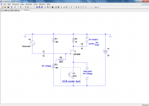
Having more or less completed the design for the npn CCS impedance test rig, I then realized that I'd probably be using PNP CCS as well so I thought simple, just turn everything on its head. However I have no p ch jfets at all, so I thought it should be possible to make a cascode with a suitably high gain PNP, in fact I have some mpsa13 small signal Darlington's, these have a minimum gain at 10mA of 5000.
I have drafted another test rig for the PNP CCS impedance measurements, see attached. Any comments / criticisms are welcome.
decent mA range cascode ccs will look like a C by even moderate/upper audio frequency
the TL07x input C will limit the measurement there
and >1 MegOhm should also be easy at DC for long channel fet, adequate bias - read the notes I linked
I have downloaded the application notes and have started reading, but I think it will take some time to fully digest, thank you for that jcx.
Having more or less completed the design for the npn CCS impedance test rig, I then realized that I'd probably be using PNP CCS as well so I thought simple, just turn everything on its head. However I have no p ch jfets at all, so I thought it should be possible to make a cascode with a suitably high gain PNP, in fact I have some mpsa13 small signal Darlington's, these have a minimum gain at 10mA of 5000.
I have drafted another test rig for the PNP CCS impedance measurements, see attached. Any comments / criticisms are welcome.
Attachments
Why not just get rid of most of the circuitry and use a simpler circuit and an oscilloscope to do the measurements? 10 MΩ input impedance. Millivolt resolution. Dunno… seems like an obvious thing to me.
The input resistors to impose a DC bias on the A/C signal source is fine. But the rest is just getting too darn complicated. Make your DC+A/C source, drive the CCS which is in series with a 1kΩ sense resistor, and get your waveforms. Dual channel scope can show both at same time. The accuracy of most scopes is somewhere between 1% and 3% unless they're particularly cheap.
Get you peak-to-peaks, haul out Excel, and input your findings. In a matter of minutes - at most - you will have a graph. Done.
GoatGuy
Why not just get rid of most of the circuitry and use a simpler circuit and an oscilloscope to do the measurements? 10 MΩ input impedance. Millivolt resolution. Dunno… seems like an obvious thing to me.
On the face of it a great idea, however my digital scopes Y amplifiers are quite noisey at maximum sensitivity getting in the way of accuracy, probably impossible to get a useful result for a signal less than or equal to 1mV sadly. My old analog 'scope that I lent to a friend would probably have been up to it.
New technology ain't always better.
I don't get what you mean: it seems that with this method, you are just going to test the CCS for its transconductance, not its output impedanceWhy not just get rid of most of the circuitry and use a simpler circuit and an oscilloscope to do the measurements? 10 MΩ input impedance. Millivolt resolution. Dunno… seems like an obvious thing to me.
The input resistors to impose a DC bias on the A/C signal source is fine. But the rest is just getting too darn complicated. Make your DC+A/C source, drive the CCS which is in series with a 1kΩ sense resistor, and get your waveforms.
I'll try this method.
With S1 closed, opening/closing S2 measures transimpedance (ie, PSRR) or output impedance. For a 2 terminal CCS they're identical. For a 3-terminal CCS like shown, they're not.
Parasitic input capacitance of amplifier is included for free in the measurements. I could either calibrate it out, or just don't care about it, since the output capacitance of the CCS is known anyway (from transistor datasheet...)
BTW, for the CCS shown, transimpedance is much worse than output impedance, unless R4 is replaced by ... a CCS ... so with this one you need a CCS to make a CCS. Its advantage, though, is that it works well with low headroom... unlike JFET.
Attachments
In sim, the darlington seems to work, at least for a simple, one-transistor CCS.Having more or less completed the design for the npn CCS impedance test rig, I then realized that I'd probably be using PNP CCS as well so I thought simple, just turn everything on its head. However I have no p ch jfets at all, so I thought it should be possible to make a cascode with a suitably high gain PNP, in fact I have some mpsa13 small signal Darlington's, these have a minimum gain at 10mA of 5000.
I have drafted another test rig for the PNP CCS impedance measurements, see attached. Any comments / criticisms are welcome.
I would be less confident for more evolved types of CCS, having a much higher impedance.
With a jFET at low frequency, you can be sure that the gate current is small and purely capacitive. The base current of Bjt's is less "clean" in this respect
Attachments
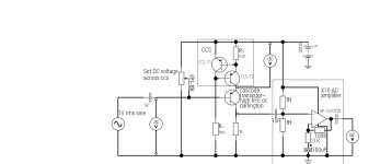
Mmm, I ended up breadboarding the npn circuit using a high gain ( hfe 450~900) transistor as the cascode transistor, but could easily swap for a jfet if anyone thinks the npn is a bad idea. I figure the base current in the cascode transistor will introduce only 0.1-0.2% error ( 1/hfe+1 )
Derivation of base current error:
Ie = CCS ac current, Ic = ac current in 1k sensing resistor.
Error=Ie-Ic/Ie
Ic=hfeIb AND Ie=Ic+Ib => Ie=hfeIb+Ib,Ie=Ib(hfe+1)
Therefore error = Ie-Ic/Ie = hfeIb+Ib - hfeIb / Ib(hfe+1)
Subtracting and dividing, ERROR = 1/hfe+1
As %, Error is 100/hfe+1
For hfe 450~900 THEN %error = (100/451)~(100/901) ~ 0.11-0.22%
See attached, I am yet to connect instruments and power up!
EDIT: final thought, do you think Ro ( 1/hoe ) in the cascode transistor will be a problem or are capacitive effects likely to dominate anyway.
Attachments
Last edited:
I would advise against that: things are more subtle than that, and even with the basic CCS, a single Bjt as cascode already shows a significant deviation.Mmm, I ended up breadboarding the npn circuit using a high gain ( hfe 450~900) transistor as the cascode transistor, but could easily swap for a jfet if anyone thinks the npn is a bad idea.
If you test better sources, it will be completely unusable
Attachments
- Status
- Not open for further replies.
- Home
- Amplifiers
- Solid State
- How do you calculate impedance of a current source?