Make yer' ground plane , have fun.🙄
Don't listen to me ...
But - look at 10 mid to real high priced "audiophile" pro - amps.
You will find my recommendations carried out to the next level ...
Full capacitor 20Kuf+ banks right on the OPS PCB with the actual main
star point right at output (on that PCB).
You won't find any ground planes (except maybe in the digital/control circuitry).
That's dual mono ...
Single large supply - big computer grade caps with copper ground rail/plate.
Short ground "runs" from speaker returns and local amp decoupling to a
single point on the common ground "bus" (adcom/hafler - 20th century
classic amps). Still no ground planes.
OS.
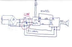
I never said star ground and looking at the high current part is not important. Remember this is only the OPS, The IPS/VAS is on a separate board. The two grounds are connect to the main resevoir cap on the chassis. It would be crazy to have one ground plane for the IPS/VAS and OPS together, as OPS have high current, you have to separate the two ground and connect to a star.Make yer' ground plane , have fun.🙄
Don't listen to me ...
But - look at 10 mid to real high priced "audiophile" pro - amps.
You will find my recommendations carried out to the next level ...
Full capacitor 20Kuf+ banks right on the OPS PCB with the actual main
star point right at output (on that PCB).
You won't find any ground planes (except maybe in the digital/control circuitry).
That's dual mono ...
Single large supply - big computer grade caps with copper ground rail/plate.
Short ground "runs" from speaker returns and local amp decoupling to a
single point on the common ground "bus" (adcom/hafler - 20th century
classic amps). Still no ground planes.
OS.
Now that I got rid of the error correction circuit, I have enough room to actually do ground cut to kind of separate the high current big transistors from the drivers and pre drivers. The OPS has a gain of less than 1, the power supply ripple is not as important as IPS and VAS. BUT the parasitic causing oscillation on the big transistor are a major problem for 3EF, having a ground plane make a day and night difference.
Attached is my preliminary grounding scheme. The start connection is on the main reservoir cap on the chassis. The ground of IPS/VAS and OPS only connect to the star ground outside. The ground from the OPS connect to the IPS/VAS board ONLY through a 51ohm resistor IF NEEDED.
And yes, I definitely use ground plane on the IPS/VAS board also.
Attachments
Last edited:
I am reading this article: Ovation e-Amp: A 180 Watt Class AB VFA Featuring Ultra Low Distortion
He talked about the thermal compensation using both the transistor in the bias spreader AND using a NTC resistor to have a dual stage thermal compensation. Is that necessary? I have seen most amps use just the transistor in the bias spreader to track the temperature of the heat sink only.
I understand the need of using two transistors for the bias spreader to keep the current through the thermal sensing NPN running constant current, the PNP is to supply the additional current during the excursion. But is it over kill using a resistor to sense the temperature?
http://hifisonix.com/ovation-e-amp/
I missed that NTC when I read about the Ovation.
It appears to be 10K in series with 7k8
This 17k8 is parallel to the two 4k7 (=2k35)
That makes the NTC effect quite subtle.
I suspect the research behind adopting this idea to be very thorough and that it would not have been implemented for no measurable benefit.
Overall the Vbe is unusually complex. It would take a lot of work with part values to adopt a similar strategy to this for your output stage.
ThanksI missed that NTC when I read about the Ovation.
It appears to be 10K in series with 7k8
This 17k8 is parallel to the two 4k7 (=2k35)
That makes the NTC effect quite subtle.
I suspect the research behind adopting this idea to be very thorough and that it would not have been implemented for no measurable benefit.
Overall the Vbe is unusually complex. It would take a lot of work with part values to adopt a similar strategy to this for your output stage.
Do I need it? I've seen a lot of schematics using just a simple NPN as Vbe multiplier. I'll be happy to adjust after it warm up to the required current. I really don't want to over complicate this. I already added a PNP to ensure the current through the NPN stay constant. I already finished the layout with the NPN of the bias circuit screw onto the heat sink already.
Thanks
Last edited:
The question I would be asking myself is:
Can I set up the NTC and the other values to be able to measure any improvement in tempco?
And my answer would be, no.
In which case it would not see any benefit to the added complication.
Can I set up the NTC and the other values to be able to measure any improvement in tempco?
And my answer would be, no.
In which case it would not see any benefit to the added complication.
Thank you, you make my day!!!The question I would be asking myself is:
Can I set up the NTC and the other values to be able to measure any improvement in tempco?
And my answer would be, no.
In which case it would not see any benefit to the added complication.
Yes, but it's long, need to play around to get the value.Has Bonzai explained his procedure to determine the tempco values?
Also, unlike the normal class AB, I am setting the current to 200mA per stage. Who cares if it is off by even 30mA!!!
Point is again, most amps don't do that. I am running the amp at higher temperature, it only going to take 10 minutes to raise the temperature to the normal operating temperature. With higher bias setting, dissipation doesn't vary as much like those that run low current. So I just wait till the amp to warm up before setting the current.
Cordell cares, Self cares.unlike normal class AB, I am setting the current to 200mA per stage. Who cares if it is off by even 30mA!!!..........
Cordell cares because of the Oliver's optimization. But in my case, I will use 2ohm even if I run 200mA each. That already violates the Oliver's optimization. So it's not that important.Cordell cares, Self cares.
I am planning to order 25 of each power transistor and group them by matching Vbe. Hopefully it is more forgiving in the thermal imbalance.
If use lower bias current and follow straight Oliver's, then yes, you care.
Last edited:
I have more questions. Now that I got rid of the error correction circuit, I have much more solid ground plane and I can afford to cut the ground to isolate the high current transistors from the pre drivers. This gives something of a star on star grounding where the ground plane for the power transistor is kind of stared.
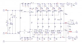
My question is which side of the ground should I put the driver Q3 and Q4 on. In the schematic, I have the rail voltage through a 22ohm resistor before powering Q20, Q21, Q3 and Q4. Since Q3 and Q4 might have bigger current when driving all the big power transistor, would it be better to move Q3 and Q4 with the power transistors before the 22ohm resistor?
I change the driver transistor Q3 and Q4 to 2SC2837 and 2SA1186 resp. since I use 5 pairs of power transistors, seems like I can use 2SC2837 and 2SA1186 even for power transistors. They have higher fT and lower input capacitance. They are still 100W transistors. What do you think?
Attached is the latest schematic.
Attachments
Last edited:
I consider the drivers as part of the output stage.
They will pass currents approaching 1Apk in medium size 8ohms amplifiers.
For lower impedance speakers and/or high power amplifiers, the driver currents will exceed 1Apk.
That puts them into the "high current" side of the amplifier.
Your 22r feeding the drivers is going to lose a lot of voltage when the amplifier is outputting high transient peak currents. The decoupling of ~110uF will satisfy some of this demand, but you are working them harder than I would.
You could download Bensen's spreadsheet that will help you analyse the output and driver SOAR.
If you want to see my modified versions, send me an Email.
Jan Didden also has an SOAR guide on his website.
If you want to see my modified versions, send me an Email.
Jan Didden also has an SOAR guide on his website.
I consider the drivers as part of the output stage.
They will pass currents approaching 1Apk in medium size 8ohms amplifiers.
For lower impedance speakers and/or high power amplifiers, the driver currents will exceed 1Apk.
That puts them into the "high current" side of the amplifier.
Your 22r feeding the drivers is going to lose a lot of voltage when the amplifier is outputting high transient peak currents. The decoupling of ~110uF will satisfy some of this demand, but you are working them harder than I would.
I kind of figure that much as I was waiting for opinions. I updated the schematic and the layout already. As you see, I moved the driver to the big transistors' side. You think this is good now? I even change to a TO-3P driver transistors that are 100W!!!
Thanks
Attachments
Last edited:
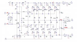
Here is the pcb layout. First one is the complete picture with power, output and ground plane in shaded mode so it's easy to see the components.
The second picture is the ground plane. Because of eliminating the error correction circuit, I have a lot more room to cut the ground. Notice the cut at the center that separate the center portion of the ground plane that contain only the pre-drivers and the bias Vbe multiplier. The left and right ground are the high current noise ground. The two grounds just connect at the center where the Power Ground (PGND) wire from the power supply connects. This serves as star on star grounding.
The second picture is the ground plane. Because of eliminating the error correction circuit, I have a lot more room to cut the ground. Notice the cut at the center that separate the center portion of the ground plane that contain only the pre-drivers and the bias Vbe multiplier. The left and right ground are the high current noise ground. The two grounds just connect at the center where the Power Ground (PGND) wire from the power supply connects. This serves as star on star grounding.
Attachments
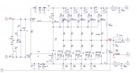
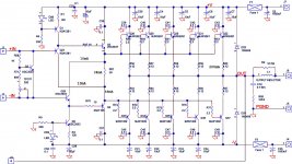
I am starting to change my mind on my version of 3EF OPS. I am tempting to do the 3EF that use one opposite transistor on each side. eg. instead of 3NPN as 3EF, I want to use PNP NPN NPN for the top half and NPN PNP PNP for the bottom half. I think there is advantage in thermal and stability of the bias multiplier circuit. Attached is the design of this. I copied from Christian ( Ranchu 32) on the the first stage. I did simulation and it did show 2dB lower 3H at 1KHz 30Vpeak output.
I feel a little uncomfortable of the two 100uF caps C1 and C9 used to keep the tail of Q21 and Q20 more of constant current. I just want comments on this circuit and what to look out for. Any down fall.
Thanks
I feel a little uncomfortable of the two 100uF caps C1 and C9 used to keep the tail of Q21 and Q20 more of constant current. I just want comments on this circuit and what to look out for. Any down fall.
Thanks
Attachments
- Status
- Not open for further replies.
- Home
- Amplifiers
- Solid State
- Please comment on my OPS design