Layout in pdf please.....
This is double side layout, pdf does not help.
Are the resistors non-inductive? If so which ones do you need, I want to buy some and the more the merrier... .22?Progress, still missing some resistors, most importantly output source resistors.
Damir
Are the resistors non-inductive? If so which ones do you need, I want to buy some and the more the merrier... .22?
The biggest problem was to find good power resistors, not to expensive non inductive, and I ordered those 200pcs 2W 0 47 Ohm 0 47R 1 Metal Film Resistors 2W Color Ring Resistance | eBay hopefully all that. I will use two in parallel.
120W-LMOSFET-CFA
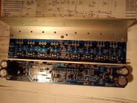
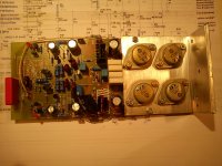
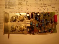
I am so slow, must be the age. Finally this is 120W lateral mosfet amp, tested with my workshop power supply, not music came yet, just bias setting and some measurement.
The main problem I encountered is input CCS. I chose the one with RED LED and that was where the problem started. Not all RED LED are with the same knee voltage, variation is quite broad. In the simulation I used Cordell's RED LED and it shows 1.65Vat 1.5 mA and a real RED LED I've bought was 1.8V-1.9V at the same current and that provoked higher CCS current and then higher VAS current and even thermal runaway. I chose that CCS because of better thermal stability, but in fact it provoked thermal instability in VAS. I think in the future I will choose simple two transistor feedback CCS, less thermally stable but with very predictable current.
Next problem is my inability to make firs time layout with no errors and I lost quite time to solve that.
Here is a photos.
I started 200W VMOSFET amp and again some layout errors are slowing me down.
BR Damir
Attachments
This is double side layout, pdf does not help.
Pdf alwayes help🙂
Double side,two pdf ,one for the top side the other for bottom.
You should mount them in the same line on that L profile I don`t think this is a good solution. Anyway, good work as always. Cheers!I am so slow, must be the age. Finally this is 120W lateral mosfet amp, tested with my workshop power supply, not music came yet, just bias setting and some measurement.
The main problem I encountered is input CCS. I chose the one with RED LED and that was where the problem started. Not all RED LED are with the same knee voltage, variation is quite broad. In the simulation I used Cordell's RED LED and it shows 1.65Vat 1.5 mA and a real RED LED I've bought was 1.8V-1.9V at the same current and that provoked higher CCS current and then higher VAS current and even thermal runaway. I chose that CCS because of better thermal stability, but in fact it provoked thermal instability in VAS. I think in the future I will choose simple two transistor feedback CCS, less thermally stable but with very predictable current.
Next problem is my inability to make firs time layout with no errors and I lost quite time to solve that.
Here is a photos.
I started 200W VMOSFET amp and again some layout errors are slowing me down.
BR Damir
You should mount them in the same line on that L profile I don`t think this is a good solution. Anyway, good work as always. Cheers!
Yes you are right, it will be better to have output mosfets in line, but I am going to use existing enclosure and that is only shape that could be squeezed inside. I have other amp JLH 80W mosfet inside similar enclosure with same two rows of output mosfets and was not problem with thermal transfer to the main heatsink. This alu L profile is 4mm thick and should be good enough, JLH uses 3mm thick with no problem. When I finish with testing I will design a new layout for the lateral mosfet in the plastic case all in one line, but again on L alu as this facilitate testing and repairing.
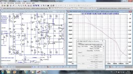
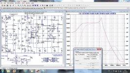
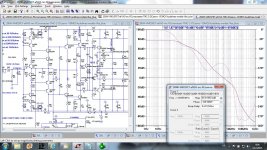
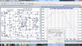
There is one question that bother me with LTspice simulation. I tried my 200W VMOSFET amp to simulate with TMC, and I did two simulation, one to check global LG, and second one to check only local compensation LG.
The global LG looks good with good PM and GM and it looks very stable on different capacitive loads, but local TMC LG shows strange phase behavior and I am bot sure how to interpret this.
This happens only if the RC was connected parallel to the VAS emitter resistor. That RC decreases THD20k from 0.000804% to 0.000365% at 50W/8ohm.
Please comment.
BR Damir
Attachments
-
 200W-VMOSFET-TMC-Tian-overall.jpg284.1 KB · Views: 685
 -
 200W-VMOSFET-TMC-David-Tian.jpg286.9 KB · Views: 653
 -
 200W-VMOSFET-TMC+RCoverVASres-Tian-overall-FFT.jpg230.1 KB · Views: 583
 -
 200W-VMOSFET-TMC+RCoverVASres-David-Tian.jpg285.2 KB · Views: 600
 -
 200W-VMOSFET-TMC+RCoverVASres-Tian-overall.jpg281.1 KB · Views: 616
The kind (size) of difference that you see is (as far as I am concerned) pretty insignificant. If you are looking for that small a difference then you must also look at the series resistance and inductance of the capacitors (and other factors, but you added a capacitor). When you arrive at the figures where you are, the test bench is the next place to be, simulation is not a replacement for measurements. For my amplifier I can get THD20k as low as 0.001083% at 250Watt into 8Ohm, now... if life was that easy 🙂
The kind (size) of difference that you see is (as far as I am concerned) pretty insignificant. If you are looking for that small a difference then you must also look at the series resistance and inductance of the capacitors (and other factors, but you added a capacitor). When you arrive at the figures where you are, the test bench is the next place to be, simulation is not a replacement for measurements. For my amplifier I can get THD20k as low as 0.001083% at 250Watt into 8Ohm, now... if life was that easy 🙂
Thank you for your comment. I am no so much concerned about distortion, bur about stability, look fourth picture and the phase behavior, that is what I don't understand, the way that jump from 0 degree to 250 degree. I would not predict that from the gain curve.
Here is quite similar simulation with different compensation and the phase behavior is quit different.
Attachments

The global LG looks good with good PM and GM and it looks very stable on different capacitive loads, but local TMC LG shows strange phase behavior and I am not sure how to interpret this.
I don't know what your 'local TMC LG' is measuring 😕 but the big jump in phase is simply the phase of a resonance.
It's much clearer if you only display phase from -180 to +180 and allow wrap around
That's simply cos you have more LG at 10kHz & above with the RC connected.This happens only if the RC was connected parallel to the VAS emitter resistor. That RC decreases THD20k from 0.000804% to 0.000365% at 50W/8ohm.
In #653, your C4,5 are 470 FARADS so you've just made R14 & P1 smaller.
In #653, your C4,5 are 470 FARADS so you've just made R14 & P1 smaller.
Sorry, that was a typing error, here is correct one, no big difference.
Attachments
There is one question that bother me with LTspice simulation...phase behavior and I am [n]ot sure how to interpret this.
Hi Damir
I have seen this previously too and have puzzled over it. Nor I can find no-one else who seems to understand it.
At first I believed it was a quirk of LTSpice but now I have come to think it does indicate a real effect.
It is difficult to interpret such plots because phase is somewhat arbitrary and I don't know how LTSpice calculates it.
The plot appears to show non-minimum phase behaviour so presumably it indicates some kind of cancellation or null caused by feed-forward, but I can't be more specific.
I suspect it is an indication that there is some undesirable behaviour that can be removed.
I have not seen it in any case where I am confident the loop is optimized.
Best wishes
David
Nice to see you put the balun to good use, now you have tried it for a while do you have any ideas for improvements I can make?
Last edited:
Are the Bin/out+ & Bin/out- terminals your Balun?Nice to see you put the balun to good use, now you have tried it for a while do you have any ideas for improvements I can make?
Hi Damir
......
Best wishes
David
Nice to see you put the balun to good use, now you have tried it for a while do you have any ideas for improvements I can make?
Hi David,
Thank you very much for the balun, now I can see better inside the compensation loop, but as you've noticed too, sometime it confuse me, not the balun but the LTspice. I don't know haw to interpret that phase behavior as it's not intuitive or obvious.
I think that my theoretical knowledge about Bode is very rusty, I studied it many years ago and now the inspiration is no more. To do that as a hobby is OK and to build some nice amps too. Sorry, no improvements from my side.
Best regards
Damir
I don't know what your 'local TMC LG' is ...
It is the Return Ratio at the VAS.
We really do need to talk "Return Ratio" because there are multiple interconnected loops so "the Loop Gain" is not well defined.
Strictly, it's the differential Return Ratio because we have used the balun to remove the common mode "noise"
... is simply the phase of a resonance.
I don't think it's this simple, look carefully at Damir's post #651, the fourth picture.
That phase is peculiar.
It's much clearer if you only display phase from -180 to +180 and allow wrap around
I think this hides the problem.
Are the Bin/out+ & Bin/out- terminals your Balun?
Yes.
Best wishes
David
Last edited:
Gasp! 😱I don't think it's this simple, look carefully at Damir's post #651, the fourth picture.
That phase is peculiar.
The mythical NMP unicorn! And at 250kHz only 😱😱
BTW, I don't think wrapping phase hides anything. In fact wrapping phase helps those versed in the art to see NMP behaviour
Last edited:
- Home
- Amplifiers
- Solid State
- 200W MOSFET CFA amp