changes done. blue pill please....🙂
Is dual layer out of the question?
We might need a ground plane now.
Is dual layer out of the question?
We might need a ground plane now.
I would like to avoid dual layer if possible, if not, so be it.
Save what you have now, to a secure place.
The Blue pill:
Disconnect R2 from ground.
Disconnect IC pins 3 and 5.
Remove caps 3,5,7,8,9 and 10
Remove R8.
Disconnect IC pin 4 from LSP5.
Remove LSP2,3,4 and 5.
Hopefully that made all the power input components and output circuitry...
Make more space behind the IC. You can have up to 4mm usable PCB area between the IC pins 2/4 and the board edge before it touches the IC heatsink.
Lets use that luxury also.
Power input capacitors. I suggest 18mm types, 2 per rail, i.e. 4pcs total.
Increase board size TO THE RIGHT and put the caps there. Power input connector where you had the speaker connection previously. The screw terminal type was OK...
Top terminal (+), mid terminal GND, bottom terminal (-).
Ceramics, former C7 between IC pins 3 and 5, put it there horizontally and as close as possible.
Under C7, put C8 horizontally. C3 vertically to the right of these. Connect to the IC and their grounds together.
Lets see what we have so far...
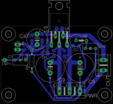
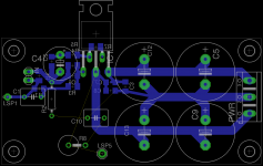
I assume you meant 8mm caps, not 18mm. Board is not able to accomodate them in a single column, so I increased the length of the board. I am not sure if you meant power connector will be to the right of the caps or the other way round. I havent done all the connections yet, just want to check if I am on the right track.
Attachments
Caps in 2 x 2 order on the right. Put their pins vertically. And yes 18mm caps. 🙂
Move C3 down to make it in line with the C7/8. Also move all the 3cap block to the right, lets say about 50mils. We shoud this way get more space for very thick leads to the chips power pins.
Move C3 down to make it in line with the C7/8. Also move all the 3cap block to the right, lets say about 50mils. We shoud this way get more space for very thick leads to the chips power pins.
Yes, but C3 the same way as you had it before. Only move it down a bit so that you have it in line with the rest...
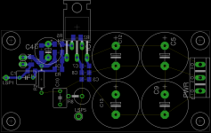
Dont rush into things... 🙂
Allmost as intended though...
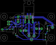
Now; I was planning to have the speaker output connector on the right of the IC close to its output pin 4. I would put a Faston spade terminal in to there (or at least pads for it, even if direct wire soldering was prefered), pitch 200mils, hole size 1,8mm.
What do you think?
Then we need also space for the R8 and C10.
C10 could be in the middle of the cap bank 5/9/12/13. We jump the positive supply rail with the R8 between Caps 5 and 12. So make PCB wider...
The power rails:
Use 45deg angle to leave the power connector exactly as you have it now, but turn to the cap later so that you dont need to put a "tee" to the pin connection point. Instead go directly to the pin. Then a direct track from C5 top pin to the C12.
Lets try with 200mil track width.
Same type of connection to the IC pin 5 as you left from the power connector.
And mirror the above for the negative rail.
Allmost as intended though...
Now; I was planning to have the speaker output connector on the right of the IC close to its output pin 4. I would put a Faston spade terminal in to there (or at least pads for it, even if direct wire soldering was prefered), pitch 200mils, hole size 1,8mm.
What do you think?
Then we need also space for the R8 and C10.
C10 could be in the middle of the cap bank 5/9/12/13. We jump the positive supply rail with the R8 between Caps 5 and 12. So make PCB wider...
The power rails:
Use 45deg angle to leave the power connector exactly as you have it now, but turn to the cap later so that you dont need to put a "tee" to the pin connection point. Instead go directly to the pin. Then a direct track from C5 top pin to the C12.
Lets try with 200mil track width.
Same type of connection to the IC pin 5 as you left from the power connector.
And mirror the above for the negative rail.
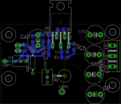
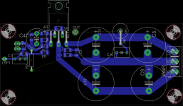
C7, the rail to rail decoupling cap, can fit between the supply pins. Are you using 805 or 1206 caps?
That allows you to move the rail to ground caps closer to the supply pins.
That allows you to move the rail to ground caps closer to the supply pins.
Andrew,
you have knowledge about the possible faulth currents in R2. I beliewe you recommend parallel/antiparallel diodes to this?
you have knowledge about the possible faulth currents in R2. I beliewe you recommend parallel/antiparallel diodes to this?
C7, the rail to rail decoupling cap, can fit between the supply pins. Are you using 805 or 1206 caps?
That allows you to move the rail to ground caps closer to the supply pins.
neither fit there. If I drop the power track width from 100 to 80, I can just squeeze in an 0603, still not enough clearance.
Is that a question?
Yes.
As you have experience with these - or do you?
You can also recommend a make and model for those - or can you?
R2 connects Signal Ground to Power Ground.Andrew,
you have knowledge about the possible faulth currents in R2. I beliewe you recommend parallel/antiparallel diodes to this?
This normally only passes interference current which should be very well attenuated.
There should be no signal current and no fault current when operating correctly.
When a fault occurs there can be mains voltage on one side of R2. This will allow Fault Current to Flow. The resistor will blow leaving one side with Mains fault still connected.
You need to provide an escape route for the Fault Current to flow to the Chassis and thence to PE.
A pair of inverse parallel power diodes do this job.
- Status
- Not open for further replies.
- Home
- Amplifiers
- Chip Amps
- please review this pcb design