There are two parasitic capacitances in the input of a common emitter (VFA-LTP) : base emitter and base collector. Plus the stray capacitances.Seems to me that VFAs equally have a pole due to stray capacitance at the -ve input. The lower impedance of this input in a "CFA" should push this pole further out.
The second point, as i explained, is a normal amplifier need an input impedance not lower than 10K. As we want the two legs of the LTP to be equal, this will be the feedback impedance, sensible to those capacitances.
In a CFA, we can make the feedback Z as low as we want, and the ouput stage is able to feed the current. This ZC pole can be out of the bandwidth of the amp, not adding a pole and increasing the slope at HF. (better stability margin)
With an optimized VFA (and a compensating cap // to the serial feedback resistance), the difference is not a big deal. It is when we look at the slew rate that the main difference appears. "Current on demand".
Hi Guys,
I am building a pair of the SlewBaby OPS boards. They are like the Slewmaster OPS except they have only 2 pair outputs and the drivers are TO-220 devices.
My question is should the current be different through the TO-220 devices than the TO-247 devices? Should I use a higher value for R113?
I'm planning to use 2SC3423-Y/A1360-Y for the predrivers and cap mutiplier, BD139 for the VBE multiliers, MJE15032/33 for the drivers and MJL4281/4302 for the outputs. It will most likely be run with +-56v rails. Does anyone see any problems with my device choices? Do you see any other components that need to be changed in the attached schematic?
Thanks, Terry
Hi Terry,
I have the baby also. I increased the r113 to 100ohms because devices mounted on a really small piece of aluminium was getting very hot. They still run hot but manageable.
My setup is BF471/472 as predriver 2sa1837/2SC4793 as drivers and MJL4281/4302 as outputs. At the beginning I had some stability issues which were fixed by inserting the extra caps on the output board.
I think your choise of devices is fine.
Jarno
It seem obvious that we want to have the open loop bandwidth of any audio amp flat in all the audio range. It means still flat at 20Khz.I think your choise of devices is fine.
This will lead to a constant feedback ratio in the band, and no, or minimal phase shift, once looped.
Unfortunately, and even with the fastest devices we can find for each stage, it is very difficult to achieve.
For me, this search for speed is the most important point, when i'm about to chose a transistor for an amp with global feedback, as well as reducing the number of stages (poles) in the loop to the minimum.
Not to talk about stability margins witch have a great impact on the sound quality during transients...
Last edited:
Hi Terry i used 47pf as csa/csb.Can't find it myself. I wouldn't even know where to start. I can certainly use very short wires once it is in an amp. Just testing right now. I have to decide which IPS will be best. On my other boards, csa/csb are not used and no problem with oscillation with any of the IPS I have built including the new Symasui I just finished. This is makeing me wonder if these transistors are my problem it the LTT4 I hav been struggling with.
Blessings, Terry
Never made serious studies about this, but, at first glance, i would try to make each stage faster than the previous,
to avoid TIM.
At the second look, if the amp is class AB, we would like to have the 'comparator' faster than the output stage to cure crossing distortion ?
My experience shows:
- Yes, fast IPS ("comparator") is always an advantage. Also, the right OLG distribution between the front-end stages is important for maintaining the low TIM (IPS is not going to be a gain champion here).
- You would also want to have the output devices as fast as possible. In EF3, for example, designing a compensation approach, it is never a good idea to slow down the "outputs" or the drivers (unless it's a really "evil" OPS). You can slow down the pre-drivers though with no problem (shunt caps).
So, in general, looking at the amp's schematic, drawn the "normal" way, it goes like this - fast left side, slower middle (this is where most of the compensation is arranged) and as fast right side as you can get (it will be slower than IPS anyway, but still).
Cheers,
Valery
Happy to see, Valery, that you correlate my 'instinctive' habits ;-)
I will add that, at the end, i tend to prefer Laterals for OPS. For two reasons: they are fast and they don't have secondary breakdown risk, making them reliable.
As i never noticed some kind of 'FET coloration' with them, i stay stuck with this technology. I like too the fact that they provide a better 'isolation' with the previous stages.
Their high impedance is an advantage too, as, most of the time, we don't need a pre-driver: Simple stages IPS, VAS and OPS are achievable, despite the high gate parasitic capacitances at HF: Simple is beautiful and good to keep the source's 'details".
For VAs, the only question that remains is Cascode or not.
For IPS and a CFB topology (that i definitively prefer after years of listening comparisons), apart CCS or not, the choice is a cap in the signal path (VSSA like), or some kind of diamond input to cure the offset. Despite the bad opinion of 'Lazy Cat' about Diamonds, based on his listening experience with this topology, i am sure that it is the way to dig. Because the extra transistor is not in the feedback loop, because it reduce the distortion at low frequencies, due to the phase shifts of the feedback cap there, because it produce a better isolation between the input line and the loop. Because it is easy to fix a low pass filter not influenced by the source's impedance.
I am interested by your comments about all those expectations.
Last edited:
AC impedance is about the value paralleled NFB resistors, usually few hundred ohms (it should be ideally equal to signal source impedance + input serial resistor- part of HF filter). In input LTP loaded with CM load those capacitancies are not issue. And cascode in LTP helps supress this completly.The second point, as i explained, is a normal amplifier need an input impedance not lower than 10K. As we want the two legs of the LTP to be equal, this will be the feedback impedance, sensible to those capacitances.
Last edited:
Happy to see, Valery, that you correlate my 'instinctive' habits ;-)
I will add that, at the end, i tend to prefer Laterals for OPS. For two reasons: they are fast and they don't have secondary breakdown risk, making them reliable.
As i never noticed some kind of 'FET coloration' with them, i stay stuck with this technology. I like too the fact that they provide a better 'isolation' with the previous stages.
Their high impedance is an advantage too, as, most of the time, we don't need a pre-driver: Simple stages IPS, VAS and OPS are achievable, despite the high gate parasitic capacitances at HF: Simple is beautiful and good to keep the source's 'details".
For VAs, the only question that remains is Cascode or not.
For IPS and a CFB topology (that i definitively prefer after years of listening comparisons), apart CCS or not, the choice is a cap in the signal path (VSSA like), or some kind of diamond input to cure the offset. Despite the bad opinion of 'Lazy Cat' about Diamonds, based on his listening experience with this topology, i am sure that it is the way to dig. Because the extra transistor is not in the feedback loop, because it reduce the distortion at low frequencies, due to the phase shifts of the feedback cap there, because it produce a better isolation between the input line and the loop. Because it is easy to fix a low pass filter not influenced by the source's impedance.
I am interested by your comments about all those expectations.
Comment: 😎🙂

THx-RNMarsh
Let's see it. Schematic?Happy to see, Valery, that you correlate my 'instinctive' habits ;-)
I will add that, at the end, i tend to prefer Laterals for OPS. For two reasons: they are fast and they don't have secondary breakdown risk, making them reliable.
As i never noticed some kind of 'FET coloration' with them, i stay stuck with this technology. I like too the fact that they provide a better 'isolation' with the previous stages.
Their high impedance is an advantage too, as, most of the time, we don't need a pre-driver: Simple stages IPS, VAS and OPS are achievable, despite the high gate parasitic capacitances at HF: Simple is beautiful and good to keep the source's 'details".
For VAs, the only question that remains is Cascode or not.
For IPS and a CFB topology (that i definitively prefer after years of listening comparisons), apart CCS or not, the choice is a cap in the signal path (VSSA like), or some kind of diamond input to cure the offset. Despite the bad opinion of 'Lazy Cat' about Diamonds, based on his listening experience with this topology, i am sure that it is the way to dig. Because the extra transistor is not in the feedback loop, because it reduce the distortion at low frequencies, due to the phase shifts of the feedback cap there, because it produce a better isolation between the input line and the loop. Because it is easy to fix a low pass filter not influenced by the source's impedance.
I am interested by your comments about all those expectations.
Richard, I'm am sure that, always walking in the same paths, we have already met us in this life or in another 🙂
Their high impedance is an advantage too, as, most of the time, we don't need a pre-driver: Simple stages IPS, VAS and OPS are achievable, despite the high gate parasitic capacitances at HF.
A very simple calculation can show how biased you are in your preferences. A 2SK1058+2SJ162 pair has a total Ciss of 1.5nF. You would need at least 2 pairs for any decent amplifier (otherwise the only 1S transconductance, 5x lower than in a vertical mosfet, will severely limit the available output current), which makes 3nF. Therefore not having an EF in between the VAS and the output stage loads the VAS with a 3nF of nonlinear capacitance (read: a non linear distortion source).
To add insult to injury, the gate stoppers (say 100ohm for each mosfet) would create a small signal pole in the forward path (again for two pairs) of 1/(3nF*25ohm*2*PI)~2.3MHz, very likely the (nonlinear) dominant pole. Here goes the ultra wide bandwidth of the CFA, not to mention you would need to compensate the gain stage at a much lower frequency (hence lower loop gain). You could of course rely on this 2.3MHz pole for frequency compensation, but then you would land deep in the PIM distortion territory. The dominant pole will wiggle with the input signal level, since Ciss is strongly dependent on the mosfet Vgd (in particular at low Vgd, that is at large output signals).
Not using an EF between the VAS and the mosfet output devices is a very bad idea for any amplifier topology. There is, of course, a good chance you won't subjectively hear these distortions (or even worse, to subjectively like them!). This is the usual excuse for crappy designs (simple, but "sounds good"), see a typical example in the VSSA.
Did-you mean schematics ?Let's see it. Schematic?
Lazy Cat's VSSA (simplest CFA, where the cap in the signal path are C4 & C6, using a CCS in the input stage):
http://www.esperado.fr/fr/temp/compare_vssa/cfa-schematic.gif
The same kind of stuff, but with a cascoded VAS:
http://www.esperado.fr/images/stories/SSA-Crescendo/ssa-crescendo-def.gif
And the diamond input:
http://www.tubecad.com/2010/05/17/Diamond Buffer Generic.png
Low pass filter, requested to ensure the slew rate of the input signal never exceed the amp capabilities, can be set between emitter of the first transistor and base of the second. The interest of this diamond stage is that the 0.7V base emitter offset of the second transistors is compensated by the inverse base emitter of the first ones. This allows both the input signal and the feedback connections (emitter of the second transistors) to be at DC 0v, no need for any isolation cap. Only the second transistor is in the feedback loop.
Of course, as the amp will have full gain at DC, more precautions have to be kept to ensure no DC offset or drift at the output of the amp, due to temperature or other mismatches.
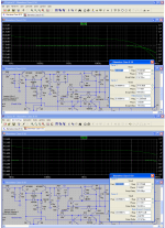
It is very simple to achieve (attachment,local NFB via R37, C20 around Q15, cascoded VAS) and the only "advantage" is increased distortion at lower frequencies (lower LG), nothing real gained at HF. In simulation with C20 connected (upper part of picture) is OLG flat to 30kHz. And as low NFB network impedance as we want-and power stage alllow (to supress influence of nonlinear parasitic capacitancies) we can use with VFA the same way as with CFA, too. No problem, only slight DC imbalance.It seem obvious that we want to have the open loop bandwidth of any audio amp flat in all the audio range. It means still flat at 20Khz.
This will lead to a constant feedback ratio in the band, and no, or minimal phase shift, once looped.
Unfortunately, and even with the fastest devices we can find for each stage, it is very difficult to achieve.
Attachments
Last edited:
Not on my experience, with a reasonable OLG, to achieve 30db of closed loop gain with enough feedback ratio for low distortion, witch was an obvious understatement.It is very simple to achieve
http://www.esperado.fr/temp/compare_vssa/open-loop-bandwith.gif
(As says Bruno Putzeys, if you use GNFB, use a lot !)
Last edited:
Possible putput devices
I am trying to compile a list of possible output devices for this design, hopefully all of the devices listed so far are appropriate. If there are any obvious mistakes, let me know.
Sanken MT-200 packages are extra wide (37mm) and will require skipping outputs on the 5 or 3 pair boards to be usable.
Toshiba: (avalable from Mouser and Digikey)
2SC5200/2SA1943 230V 150W 30MHz TO-264
2SC5242/2SA1962 230V 130W 30MHz TO-3P
Fairchild: (avaliable from Mouser and Digikey)
FJL4315/FJL4215 Toshiba 2SC5200/2SA1943 copy 250V
FJA4313/FJA4213 Toshiba 2SC5242/2SA1962 copy 250V
On Semi: (avalible from Mouser, Digikey, and Newark/Farnell)
NJW0281/NJW0302 250V 150W 30MHz TO-247
NJW3281/NJW1302 250V 200W 30MHz TO-247
MJL3281/MJL1302 250V 200W 30MHz TO-264
MJL4281/MJL4302 250V 230W 30MHz TO-264
MJL21193/MJL21194 250V 200W 4MHz TO-264
Semelab: (avalible from Profusion and Newark/Farnell)
MG6330/MG9410 230V 200W 35MHz TO-3P
MG6330-R/MG9410-R 260V 200W 35MHz TO-3P
MG6331/MG9411 230V 300W 35MHz TO-3P
MG6331-R/MG9411-R 260V 300W 35MHz TO-3P
MAG6332/MAG9412 230V 400W 35MHz TO-264
MG6333-R/MG9413-R 260V 400W 35MHz TO-264
Sanken: (available from Digikey and Profusion)
2SC3263/2SA1294 230V 130W 35MHz MT-100/TO-3P
2SC3264/2SA1295 230V 200W 35MHz MT-200
2SC3519/2SA1386 160V 130W 40MHz MT-100/TO-3P (70V rails max)
2SC2922/2SA1216 160V 200W 40MHz MT-200 (70V rails max)
2SC6145A/2SA2223A 260V 160W 35MHz MT-100/TO-3P
Can I ask a question about the Sanken MT-200 packages now being talked about. Is it only the actual package width that is the problem with using these devices and the current pcb layout with the limitation of device spacing that we are ta;king about? I am planning on using a secondary angled aluminum angle to mount the devices at a 90 degree angle to the board surface which would allow the devices to be spaced with two of these angles per side so that the devices are staggered from each other. Is there a real gain in using these MT 200 devices if the spacing can be overcome? What are the actual advantages to using these devices?
The angled aluminum brackets would be mounted to a normal heat sink that would be parallel to the pcb, this will allow me to use a narrower heat sink than would normally be used, the heat sink will be mounted vertically with the fins running in the vertical direction and will be about 14" or 300mm high. The width of the heat sink is limited to about 4" or 100mm in my design.
The angled aluminum brackets would be mounted to a normal heat sink that would be parallel to the pcb, this will allow me to use a narrower heat sink than would normally be used, the heat sink will be mounted vertically with the fins running in the vertical direction and will be about 14" or 300mm high. The width of the heat sink is limited to about 4" or 100mm in my design.
I am trying to compile a list of possible output devices for this design, hopefully all of the devices listed so far are appropriate. If there are any obvious mistakes, let me know.
Sanken MT-200 packages are extra wide (37mm) and will require skipping outputs on the 5 or 3 pair boards to be usable.
Sanken: (available from Digikey and Profusion)
2SC3263/2SA1294 230V 130W 35MHz MT-100/TO-3P
2SC3264/2SA1295 230V 200W 35MHz MT-200
2SC3519/2SA1386 160V 130W 40MHz MT-100/TO-3P (70V rails max)
2SC2922/2SA1216 160V 200W 40MHz MT-200 (70V rails max)
2SC6145A/2SA2223A 260V 160W 35MHz MT-100/TO-3P
Most of these Sanken devices are available through Newark also and they are on sale right now.
I noticed a mistake on MJL4281/4302 they are 350V devices with 35MHz fT.
Good to know, I forgot to check Newark/Farnell for Sanken devices when typing out my post.
Yes, the only problem is the width of the package. The advantage to Sankens is mainly the better specs, their reputation for sounding good certainly doesn't hurt either...
Your idea with mulitiple angle brackets could work, but don't forget Q104 must be attached to the same heatsink as the outputs. The closer Q104 is (thermally) to one of the outputs the better.
Most of these Sanken devices are available through Newark also and they are on sale right now.
Good to know, I forgot to check Newark/Farnell for Sanken devices when typing out my post.
Can I ask a question about the Sanken MT-200 packages now being talked about. Is it only the actual package width that is the problem with using these devices and the current pcb layout with the limitation of device spacing that we are ta;king about? I am planning on using a secondary angled aluminum angle to mount the devices at a 90 degree angle to the board surface which would allow the devices to be spaced with two of these angles per side so that the devices are staggered from each other. Is there a real gain in using these MT 200 devices if the spacing can be overcome? What are the actual advantages to using these devices?
The angled aluminum brackets would be mounted to a normal heat sink that would be parallel to the pcb, this will allow me to use a narrower heat sink than would normally be used, the heat sink will be mounted vertically with the fins running in the vertical directibon and will be about 14" or 300mm high. The width of the heat sink is limited to about 4" or 100mm in my design.
Yes, the only problem is the width of the package. The advantage to Sankens is mainly the better specs, their reputation for sounding good certainly doesn't hurt either...
Your idea with mulitiple angle brackets could work, but don't forget Q104 must be attached to the same heatsink as the outputs. The closer Q104 is (thermally) to one of the outputs the better.
akkimet,
Thanks for the answer. I don't think that the Q104 should be a problem and all the outputs will share a common major heat sink, they just have to go through an intermediary connection to that sink.
Thanks for the answer. I don't think that the Q104 should be a problem and all the outputs will share a common major heat sink, they just have to go through an intermediary connection to that sink.
- Home
- Amplifiers
- Solid State
- Slewmaster - CFA vs. VFA "Rumble"