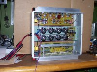
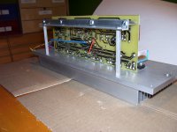
I thought about a two-box construction but the PSU on the bottom presented a good line of convection to the "hot box" of the actual circuit/transistors. It runs very cool; I am thinking of upping the bias to keep it in class A longer, see if it changes the sound...
Oh and thanks for the complement: as the creator of something less than pretty (though highly functional and Cheap) I very much appreciate a "nod" 🙂
Oh and thanks for the complement: as the creator of something less than pretty (though highly functional and Cheap) I very much appreciate a "nod" 🙂
Well, go for 100-120mA bias or even 150mA if under normal listenning conditions it does not get hot.
When it comes to boxing old PC cases are almost ideal to house PAs. Such a case also provides some transformer screening.
It is also worth adding overcurrent protection. It may happen that one of the speker terminals gets loose, falls out and creates a short on a speaker box terminal.
cheers,
When it comes to boxing old PC cases are almost ideal to house PAs. Such a case also provides some transformer screening.
It is also worth adding overcurrent protection. It may happen that one of the speker terminals gets loose, falls out and creates a short on a speaker box terminal.
cheers,
Cool janusz. I'll keep and eye out for a good PC case at my favorite recycler.
I'll report back the results of my increased bias too for anyone interested.
As to the overcurrent protection I don't actually know what you mean. I understand a fuse; do you mean I should consider a fuse on the speaker terminals?
Cheers!
I'll report back the results of my increased bias too for anyone interested.
As to the overcurrent protection I don't actually know what you mean. I understand a fuse; do you mean I should consider a fuse on the speaker terminals?
Cheers!
overcurrent protection
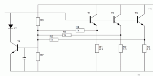
As ostripper did not make it part of the design it has to be added on a separate board.. Design and calculation algorithms were provided by audiofan in this or the other HB thred.
Circuit diagram attached but you have to calculate resistor values for your particular values of output emitter resistors (0.22 ohm in the original HB design).
If you dont find audiofan posts in this or the other thread I'll post mine tomorrow. I have 0.18 ohm emitter resistors.
cheers,
Attachments
janusz, thanks!
My emitter resistors are nominal .22R but measure .2R
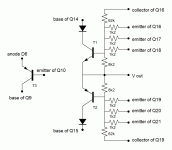
Forgive my ignorance but what are T1, T2 and T3?
My emitter resistors are nominal .22R but measure .2R
Forgive my ignorance but what are T1, T2 and T3?
T3 is limiting current through VAS when protection circuit is activated. You may solder it to the other side of the board. The reminder of the current limiting circuit needs its own board. Attached file shows calculations. These are done for 1k resistors in my HB version.
Diodes protect T1 and T2 transistors from negative/positive voltages that can be present when the other side of the output stage is conducting. A capacitor (10-47uF) can be added between the base of T1 (and the other for T2) and the output. It slows down the circuit reaction to allow higher current for brief periods of time.
cheers,
Attachments
Last edited:
careful, the 8k2 don't look like the right values.
Agree; My maths suggest R7 at 1k6 (if Vbe = 0.65V) gives a better fit on the de-rated SOA for an MJL4281.
Janusz,
R8 should be 56k (334//3100=301)
For the sake of a resistor and a diode each side, a better dual slope arrangement can be effected.
Brian.
Apologies in advance for asking something that i'm sure has been asked previously. But is this amplifier (or any other ~100-150w@8ohm output stereo power amps like this one) available in a complete kit with, boards, power supply, components, etc included.
current limiter resistor values
Values on the diagram are just examples. Possibly OK for chosen emitter resistors and chosen voltages.
With 1k resistors going to emitters, 0.18 ohm emitter resistors and 120V I get R7=3.1k (0.65V/0.21mA);
and with R8 you are right (334||3100 = 301) so R8=56k (120V/2.16mA). If you see any other error in my calsc Brian, please point it to me. I'm using ss9014 transistors in the limiter and my output transistors are MG6331/9411.
When I made my choices for emitter resistor values (0.18 ohm) I did not think about adding a current limiter. Ony when I blew two output transistors i believe due to short circuiting the output I started to think about it.
Lower emitter values reduce distortion, higher values make it easier for current limiter to operate and thermal stability is easier to achieve.
cheers,
PS attached is Excel spreadsheet (Transistor Load Lines) I wrote long time ago but the shown calcs are for HB
Attachments
Last edited:
Janusz,
post1267 .doc
where is the schematic that shows the components coding/numbers?
#1239
kemicalx, you can assemble all you need by going to the DIYaudio store for the boards and casework then your favorite electronics site for the components from the BOM (or bill of materials). It's two-stop shopping instead of one; not bad at all!
The capacitor allows a different transient current limit, from the DC current limit.
A good IV protection system will allow all valid audio signals to pass into all valid audio loads.
If the IV system cannot meet that basic requirement, then it will be audible.
As a starter, look at what the limiting locus looks like when Vbe of the protection transistor is ~ 400mVbe, i.e. just turning on.
Last edited:
Power board layout question
Which performs better with a center tap transformer?
1). This?
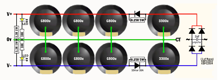
2). Or, This?
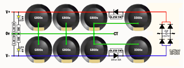
P.S.
Before I forget, I'd like to ask an additional question. Where is the most ideal location for the drainer/led section (and optional snubbers)?
A). As shown, or. . .
B). Drainer load put right after the R||D series element?
C). Drainer load put right before the R||D series element?
*As for audio quality, I might tend to guess C, because closest to bridge rectifier, but I'm not certain.
Which performs better with a center tap transformer?
1). This?
2). Or, This?
P.S.
Before I forget, I'd like to ask an additional question. Where is the most ideal location for the drainer/led section (and optional snubbers)?
A). As shown, or. . .
B). Drainer load put right after the R||D series element?
C). Drainer load put right before the R||D series element?
*As for audio quality, I might tend to guess C, because closest to bridge rectifier, but I'm not certain.
Attachments
Personally, I would expect 1) to be preferred in your choices. All PCB traces have resistance proportional to their length (for a given width and thickness). Option 2) has additional 0V trace length in series with the 3300uF capacitors, and consequent series resistance, which would tend to slightly reduce their peak current smoothing ability.
As for the remainder of the circuit, it resembles a 3-stage pi-filter. I suppose the circuit could be simulated by inserting small equivalent resistance values in proportion to trace CSA & lengths.
As for the remainder of the circuit, it resembles a 3-stage pi-filter. I suppose the circuit could be simulated by inserting small equivalent resistance values in proportion to trace CSA & lengths.
for me, tie all caps together for the positive and negative rails, and make them meet the center tap pad in one place....
what is the purpose of the resistor and the diode?
what is the purpose of the resistor and the diode?
- Home
- Amplifiers
- Solid State
- diyAB Amp - The "Honey Badger"