As noted in my LM3886 Bypassing Revisited Thread, the supply impedance is dominated by the resistance of the connectors and wires at frequencies below 1 kHz. In the mid audio band (1~10 kHz), the impedance is dominated by the ESR, ESL of the on-board electrolytic can. My simulations show that 470~1000 uF is about optimum. I saw minuscule improvement when going from 1000 uF to 10000 uF. Above 10 kHz, the supply impedance is determined by the local bypassing network (C1, C4, C13, C16 in my circuit).
Basically, this says that a regulated supply will provide a benefit at frequencies below 1 kHz. Above 1 kHz, the performance is determined by the on-board components. The improvement I measure at 20 kHz is real and must be caused by the on-board components or layout changes. I used the same generic 1000 uF, 10 uF, and 47 nF caps that I used in my previous PCB and P2P experiments, hence, the improvement must be from the layout.
The new layout improves five things:
My guess is that the better grounding and elaborate use of planes and pours is responsible for the improvement at 20 kHz. The overall improvement across the entire audio band is caused by better grounding. See page four-ish of this thread for my grounding experiments.
Parasitic inductance in R1? Compared to my previous layout, there's probably an additional 30 nH of inductance in series with R1. Does this impact the performance at 20 kHz? Let's run the numbers: XL = 2*pi*f*L --> XL = 2*pi*20E3*30E-9 = 3.77 mΩ. This is negligible compared to the 1 kΩ resistance, hence, the parasitic inductance in series with R1 is not responsible for the improvement in THD at 20 kHz.
Regulated supply? There's no doubt that keeping the charging pulses off the board will have an impact on the performance of the amp. The question is how much charging current one would see if using reservoir caps of, say, 22000 uF off the board and routing a heavy wire to the board. My guess is that around 1/22 of the current would run through the caps on the board. How much crap this introduces is a good question. I do plan to measure this...
That said, regulated supplies are rather inexpensive, so why bother with the heavy transformers?
~Tom
Basically, this says that a regulated supply will provide a benefit at frequencies below 1 kHz. Above 1 kHz, the performance is determined by the on-board components. The improvement I measure at 20 kHz is real and must be caused by the on-board components or layout changes. I used the same generic 1000 uF, 10 uF, and 47 nF caps that I used in my previous PCB and P2P experiments, hence, the improvement must be from the layout.
The new layout improves five things:
- The supply inductance is much, much lower due to the use of planes for the supply lines.
- The decoupling has moved as close to the LM3886 as possible.
- The ground connections of the decoupling caps have been placed as close to each other as possible. This to get as close to a star ground as possible, thereby, controlling the HF current flow in the ground plane.
- The parasitic inductance of the Zobel network has been greatly reduced and its ground connection has been moved to as close to the star ground as possible.
- R1 has moved off the star ground and is grounded at the load ground. This should minimize the impact of any error signal introduced between the load ground and the star ground.
My guess is that the better grounding and elaborate use of planes and pours is responsible for the improvement at 20 kHz. The overall improvement across the entire audio band is caused by better grounding. See page four-ish of this thread for my grounding experiments.
Parasitic inductance in R1? Compared to my previous layout, there's probably an additional 30 nH of inductance in series with R1. Does this impact the performance at 20 kHz? Let's run the numbers: XL = 2*pi*f*L --> XL = 2*pi*20E3*30E-9 = 3.77 mΩ. This is negligible compared to the 1 kΩ resistance, hence, the parasitic inductance in series with R1 is not responsible for the improvement in THD at 20 kHz.
Regulated supply? There's no doubt that keeping the charging pulses off the board will have an impact on the performance of the amp. The question is how much charging current one would see if using reservoir caps of, say, 22000 uF off the board and routing a heavy wire to the board. My guess is that around 1/22 of the current would run through the caps on the board. How much crap this introduces is a good question. I do plan to measure this...
That said, regulated supplies are rather inexpensive, so why bother with the heavy transformers?
~Tom
Tom, thanks for the extensive reply.
1-4 I can understand and are all improvements on the first PCB and P2P designs.
Its Point 5. I am still trying to understand why connecting R1 (Ri) to input GND is an improvement on connecting R1 separately to the load ground. You have already demonstrated with the P2P tests that IN+FB long GND is the best version.
I was estimating the inductance at 120 nH (20 nH resistor + 100 nH trace). But this still doesn't explain the improvement at 20 kHz.
I don't have a latest layout to refer to but it sounds like the INPUT CIRCUIT layout and connections are critical to getting best performance.
The INPUT CIRCUIT is a two wire system from input socket to amplifier input pads.
In between we have some filtering, but it is still a TWO WIRE connection.
Rin, presumably the High value resistor determining the input impedance seen by the Source, MUST return to the input socket. It MUST NOT go to the Main Audio Ground.
For the past couple of months (just pre-dating Tom's p2p vs PCB experiment) I have been pondering starting a "amplifier Wiring LAYOUT guide"
Hand drew all the sketches but knowing the effort required to convert them to CAD drawing, have put off.
Maybe just photograph the hand drawings and post the guide anyway?
Hand drew all the sketches but knowing the effort required to convert them to CAD drawing, have put off.
Maybe just photograph the hand drawings and post the guide anyway?
Maybe just photograph the hand drawings and post the guide anyway?
It will be good enough for everyone around here...just open your own thread please, thank you.
AndrewT,
If you want some cad drawings made I'll have a go. Can even simulate in Lspice, It could lead to some good discussions and better understanding.
Are we talking about Rin or Ri?
http://www.diyaudio.com/forums/chip-amps/252436-lm3886-pcb-vs-point-point-data-3.html#post3846783
I think this is the best description and schematic so far. Version IN+Ri long GND.
Last edited:
Its Point 5. I am still trying to understand why connecting R1 (Ri) to input GND is an improvement on connecting R1 separately to the load ground. You have already demonstrated with the P2P tests that IN+FB long GND is the best version.
Treating IN+ and IN- as a differential pair essentially implements something akin to remote sensing in a power supply. The LM3886 will track the voltage between the input "hot" and input "cold" (avoiding the terms "signal" and "ground" here). You need to make sure that V(hot)-V(cold) is as close to the input voltage as possible. Bringing R1 back to the input connector eliminates the error term otherwise present between V(cold) and the RCA shield.
The improvement at 20 kHz must be from the planes. It's not from R1.
I don't have a latest layout to refer to but it sounds like the INPUT CIRCUIT layout and connections are critical to getting best performance.
Yep. The latest layout is in Post #210.
The INPUT CIRCUIT is a two wire system from input socket to amplifier input pads.
In between we have some filtering, but it is still a TWO WIRE connection.
Rin, presumably the High value resistor determining the input impedance seen by the Source, MUST return to the input socket. It MUST NOT go to the Main Audio Ground.
However... At some point you must refer to the Main Audio Ground. Otherwise, the signal source could drive the LM3886 outside its allowed common mode voltage range. That would result in fireworks (providing a low enough drive impedance).
~Tom
For the past couple of months (just pre-dating Tom's p2p vs PCB experiment) I have been pondering starting a "amplifier Wiring LAYOUT guide"
Hand drew all the sketches but knowing the effort required to convert them to CAD drawing, have put off.
When I started reading the ChipAmps forum, I was a bit surprised by the amount of trouble people were having with the LM3886. I was also a bit put off by the "Thou shalt [implement these changes]. So it was written and so it shalt be done"
approach that I saw from people trying to help. It seemed as if a design guide was needed.
I'm all too keenly aware of how much work it takes to put together a good website. My approach was to start writing and just chip away at the task little by little. Here's what I have so far: Taming the LM3886 Chip Amplifier, Neurochrome :: Audio.
The page is work in progress. That's why you don't find it linked anywhere (except here).
My goal is to have a guide that seriously stretches the thinking of the absolute beginner. Hopefully, they'll read some of the references and gain understanding. For the advanced DIY'er, my site should provide a comprehensive guide. For the experienced engineer, it should (hopefully) be mostly review, but still useful.
Rather than "you must", I state the tradeoffs, my preferred solution, and - most importantly - why I believe that's the best solution.
~Tom
Treating IN+ and IN- as a differential pair essentially implements something akin to remote sensing in a power supply. The LM3886 will track the voltage between the input "hot" and input "cold" (avoiding the terms "signal" and "ground" here). You need to make sure that V(hot)-V(cold) is as close to the input voltage as possible. Bringing R1 back to the input connector eliminates the error term otherwise present between V(cold) and the RCA shield.
~Tom
So its more important to connect Ri and Rin to the input GND than connecting Ri to the output GRD.
Your explanation is clear, thanks.
Bruno "The Man" Putzeys wrote a very interesting article in Linear Audio entitled "The G Word" where he strongly advocates the use of opamps as difference amplifiers.
For example, in this schematic :
Differential amplifier - Wikipedia, the free encyclopedia
You would wire :
The two inputs V1 and V2, to audio input "hot/cold" (input connector signal and shield if RCA)
Out to loudspeaker "+"
The "GND" symbol in the schematic is actually a ground sense input, wire it to loudspeaker "-"
Note this makes your amplifier inverting, which is a Good Thing (it eliminates common mode distortion in the input stage).
However, you need precision matched resistors for good CMRR. Fortunately :
DigiKey provides
And the driving source's output impedance is part of the CMRR. So you need a buffer. This is equivalent to making a 3-opamp instrumentation amplifier with the LM3886 as the output opamp. If you put, say, a DAC, or a preamp, inside the same box as your LM3886 amps, this comes for free, though. Since most DACs have balanced out, usually followed by a differential to single ended filter/conversion, if you fancy digital volume control, you can delete the final opamp and replace it with LM3886...
Then, GND noise is reduced in the output by the CMRR of the whole thing. Even if it's only 40dB, it is still 40dB better than star ground...
Last edited:
Bruno "The Man" Putzeys wrote a very interesting article in Linear Audio entitled "The G Word" where he strongly advocates the use of opamps as difference amplifiers.
Using differential circuitry is a good way to avoid ground issues for sure. However, note that if you are using regular ±5 % or even ±1 % tolerance resistors, the resulting CMRR is actually not very good. ±1 % would result in 40 dB of CMRR. That's better than nothing, but far from stellar. For input buffers, I would use one of the dedicated differential receivers such as the THAT1200-series.
For example, in this schematic :
Note this makes your amplifier inverting, which is a Good Thing (it eliminates common mode distortion in the input stage).
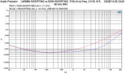
There's much drama about inverting versus non-inverting. Some go as far as indicating that if the LM3886 is used as a non-inverting amp, it will basically be useless. I strongly disagree.
First off, the difference in THD between the inverting and non-inverting is practically negligible (see attached results - I measured this using an AP SYS-2700). Secondly, the resulting low input impedance of the inverting configuration means that the amplifier will need an input buffer. Now the designer will have to manage the grounding between the op-amp buffer and the LM3886. As we know, there are many ways to screw that up.
My recommendation is to use a non-inverting LM3886 unless you have the design skills (and test equipment) to do the job right (and verify your work).
Ouch... So for $7.50 I get to build my own diff amp. Even I somehow managed to get the layout completely matched, I'd still only get 66 dB of CMRR as the resistor matching is "only" ±0.05 % (that's actually quite good).
...or I could spend $5.55 on a THAT1200 and get 90 dB CMRR.
~Tom
Attachments
Last edited:
Mmm, y'all might want to look a little closer. Difference amp CMRR is proportional to gain (see equation 3) so with the ORNTA array you link the basic result would be 86 dB CMRR min. Which is functionally equivalent to the 90dB CMRR typ of THAT's tightly trimmed parts. The lower impedances in the ORNTAs may result in more temperature related degradation (a 5 ppm tracking TCR is a 0.005% matching error per degree C, so it doesn't take much Joule heating to degrade 0.05% matching) but THAT does not specify this characteristic for their parts. So one would have to measure.Even if it's only 40dB, it is still 40dB better than star ground...
A more flexible design option is 0.05% and 0.1% Susumu RG resistors, which are cheaper than ORNTAs but lack a tracking TCR guarantee. Both are most commonly available in 25 ppm TCR. So, given the tight layout needed to not faff up the difference amp's impedance matching, one can probably manage enough thermal coupling between, say, 0805 RGs to do better than that. Wouldn't count on getting Vishay's guaranteed 5 ppm tracking TCR or THAT's likely comparable tracking.
With either of these options implementing the input buffer of the three op amp instrumentation formed with the power amp difference amplifier is nontrivial. A goodly number of audio op amps aren't specified for input impedance and, among ones which are, often no indication is made as to whether it's a common mode or differential specification. National, er, TI's LME497xx series is an exception at 1M common mode. Which, if you put them to the same test cases THAT uses, is 70dB CMRR. At which point, well, 0.5% Susumu RR resistors in the diff amp around the chip amp are pretty well good enough. And they cost maybe an extra cent each. One can JFET on this or copy THAT's bootstrap circuit but, as tomchr points out, the 10M input impedance of the THAT 1200 family offers excellent value here. The AD8421 is one of the few dedicated instrumentation amplifiers suitable for audio use. Its B grade does beat the 1200s but runs around a 60% cost riser and is harder to front with an RFI filter.
However, for the integrated DAC and power amp cases you mention parts like the THAT 1240 are perhaps more interesting. They're cheap for the resistor matching and performance you get and most such applications want the differential DAC output to single ended power amp feedback loop a difference amplifier provides. In particular, THAT specifies the 1246 at 90dB CMRR typ with a -6dB gain. So, if one hooks it up backwards to get 6dB gain off a DAC output, it's 102dB CMRR. If extreme sports are your thing implementing the DAC analog lowpass filter and laying out the DAC+chip amp PCB to realize that performance is a very interesting challenge.
Ill posed question as the requirements are inadequately specified. 😉
I think what you may be trying to ask is how much input CMRR is needed to avoid subjective degradation when translating between reference voltages. If so, the answer is anywhere from 0 to 100dB works well depending on circumstances. This thread likely sets a record for characterizing the different options along the design continuum. So there's plenty of data here to reason over when selecting an implementation.
I think what you may be trying to ask is how much input CMRR is needed to avoid subjective degradation when translating between reference voltages. If so, the answer is anywhere from 0 to 100dB works well depending on circumstances. This thread likely sets a record for characterizing the different options along the design continuum. So there's plenty of data here to reason over when selecting an implementation.
Mmm, y'all might want to look a little closer. Difference amp CMRR is proportional to gain (see equation 3) so with the ORNTA array you link the basic result would be 86 dB CMRR min.
/me thinketh thy math is broken... Equation 3 says:
CMRR = (1+Ad)/(4*t), where Ad is the differential gain and t is the resistor tolerance.
The resistor array linked to above offers 0.05 % matching --> t = 0.0005. Hence, the worst case CMRR (assuming Ad => 1) is 2/0.002 = 1000 (= 60 dB).
Good article, though.
The lower impedances in the ORNTAs may result in more temperature related degradation (a 5 ppm tracking TCR is a 0.005% matching error per degree C, so it doesn't take much Joule heating to degrade 0.05% matching) but THAT does not specify this characteristic for their parts. So one would have to measure.
That effect would be signal dependent as well. I would expect to see a THD degradation from the TCR as well.
If the process THAT uses for their audio chips is of any value as a precision audio process, it should include a TFR (thin-film resistor) module. Typically, the TCR of TFR is very, very low (commonly claimed to be zero, but there's probably a few ppm or ppb there...) The TFR modules tend to be optimized for matching and low TCR.
Anyway. My point is that I would expect the THAT chips to meet or (more likely) beat the discrete resistor module on TCR.
Just looking to turn all this theory in to a practical design.
I'm not stopping you... 😉
~Tom

Hi ! I mentioned the differential circuit as "food for thought", not "you must do it like this or you're an idiot" 😉
But... the elephant in the room for a simple substractor opamp is the output impedance of whatever is before (ie, the opamp buffer and all the wiring)... integrated diff receivers like the THAT have a huge advantage here.
The resistor array linked to above offers 0.05 % matching --> t = 0.0005. Hence, the worst case CMRR (assuming Ad => 1) is 2/0.002 = 1000 (= 60 dB).
But... the elephant in the room for a simple substractor opamp is the output impedance of whatever is before (ie, the opamp buffer and all the wiring)... integrated diff receivers like the THAT have a huge advantage here.
- Home
- Amplifiers
- Chip Amps
- LM3886 PCB vs Point-to-Point (with data)