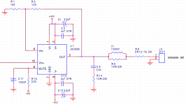
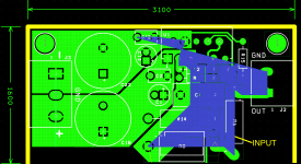
Here's what I have in mind for the optimized board. I've shown the LM3886 part of the board, hence, the flailing input trace. Green = top layer; red = bottom layer.
Ground is a plane on the bottom and VCC, VEE and the pin 3 output are poured as planes as well. That should provide a low resistance, low inductance path for the current to flow.
The decoupling will be 4.7 uF X7R ceramic + 22 uF OSCON + 1000 uF electrolytic. The latter is not shown in the schematic but is pretty obvious in the layout. Curious why, check out my LM3886 Bypassing Revisited Thread.
I have yet to settle on the final values for the Zobel network, so don't get your underwear in a bunch just because the values on the schematic don't suit your fancy.
~Tom
Attachments
Hi Tom,
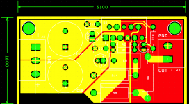
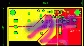
I hate to say this, but layout doesn't look right to me...see images for positive and negative going HF loops...they are to big and on the wrong side of the pcb.
I hate to say this, but layout doesn't look right to me...see images for positive and negative going HF loops...they are to big and on the wrong side of the pcb.
Attachments
Last edited:
I think the supply routing is quite excellent and much better than the average, it is always possible to find a very low loop area HF current path as well as a highly conductive one. Charge currents and load currents are seperated, the main audio GND (reference for feedback) is right at the chip. For a single amp or a dual mono build this is a good solution.
I agree one might dig in even further in the effort of separating and minimizing loops, compacting the bypassing, and have all loops designed for neglegible mutual coupling but this can easily get academic, with the chip itself dominating distortion/noise once the layout is "good enough" which this one is certainly close to as is.
A potential real problem I see is the routing of the output trace alongside the positive chip supply that will promote inductive coupling of halfwave-rectified high load current that won't be corrected by feedback because this happens outside the loop.
This is the loop for the output current, having nothing to do with supply and decoupling loops. IME output loop area / inductance (after feedback / reference nodes) is not a problem unless you have magnetic strong fields nearby. The L//R opens it up for HF anyway so there can't be any strong parasitic coupling either.I hate to say this, but layout doesn't look right to me...see images for positive and negative going HF loops...they are to big and on the wrong side of the pcb.
A potential real problem I see is the routing of the output trace alongside the positive chip supply that will promote inductive coupling of halfwave-rectified high load current that won't be corrected by feedback because this happens outside the loop.
If pin 3 is the output pin and pin 1(pin 5 also) is the positive supply so they're already very close so how can one avoid inductive coupling between the two especially if the rest of the leads (after soldering) is long enough to cause the coupling?
You are right, once the length of those PCB tracks is comparable to, or even shorter than chip lead length it isn't of significance any more. Note, though, that the feedback is taken after the coupling along the chip's leads so feedback will help reduce any effects.
In Tom's slightly asymmetric layout the GND plane will help cancel some of the field of the pos rail current but I still tend to get excited whenever I see tracks carrying rectified currents running really close along signal lines.
In Tom's slightly asymmetric layout the GND plane will help cancel some of the field of the pos rail current but I still tend to get excited whenever I see tracks carrying rectified currents running really close along signal lines.
Last edited:
It looks like there's no need for me to comment about the HF loops. KSTR made my point quite nicely. Thanks.
On the coupling between the VCC and OUT, yeah... that did concern me when I drew the pours. I was mostly looking at the fringe cap (which should not be relevant for AF). I don't have a good model in my head for the mutual inductance. I s'pose I could dig out a calculator for that.
That said, more spacing between VCC and OUT would not hurt as long as there's plenty of copper on both. I'm considering getting a different cap for C8 (Zobel cap). Currently, there's room for a sizable polypropylene unit there. A polyester cap would be smaller and do the job just as well. PP caps are getting harder to find in smaller footprints it seems... They do make good snubber caps, though, thanks to their low ESL. A physically smaller C8 would allow more space for the VCC pour and still leave enough space between VCC and OUT.
I have one concern. I'm not sure if it's valid. The feedback resistor, R1, connects to the ground plane. It's pretty close to where I expect the "star ground" in the ground plane to be (roughly centered between the decoupling caps). It should be OK, and I plan to etch the board with that configuration, but I wonder if a separate ground trace to the ground pin of one of the decoupling caps would be better. That's pretty easy to try once I have the board done, though. Just cut the spokes in the thermal relief and run a wire. No biggie... I'll do that. That's what prototypes are for... 🙂
Thanks for your comments. I appreciate it.
~Tom
Last edited:
I am surprised this PCB version doesn't follow the P2P version, but this is far more exciting....
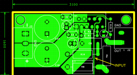
Tom, I'd rather move that Main Audio Ground more to the right side. That's where the feedback references to and the farer away from anyI have one concern. I'm not sure if it's valid. The feedback resistor, R1, connects to the ground plane. It's pretty close to where I expect the "star ground" in the ground plane to be (roughly centered between the decoupling caps). It should be OK, and I plan to etch the board with that configuration, but I wonder if a separate ground trace to the ground pin of one of the decoupling caps would be better.
disturbing high currents the better. The output of the driving circuit references to the low right section of the plane, right? If so, one more reason to isolate the MAG from rail and ouput currents. To illustrate my point (and wrt previous post) I colored the PCB artwork for audio-frequency positive output and rail current by trying to draw what the current centroids will be, and marked the MAG with a orange dot. I fear that the curl in pos rail current could introduce eddy current disturbance of the MAG for the positive load current, at least a different one than on the negative side (not shown but easy to figure out that it is way different).
Have fun and keep tweaking 🙂
Attachments
I am surprised this PCB version doesn't follow the P2P version, but this is far more exciting....
In my experience on IC layouts, connect-the-dots layouts provide far worse performance that a well thought-out layout due to higher parasitics, coupling into sensitive nodes, and lack of control of the current flows. The "3D routing" possible with P2P does not translate well to a PCB and most layouts end up in a hairball because of this. To fit all the ground traces, the components have to be spread apart, which increases the loop area and trace inductance.
My aim with this layout is to match the performance of the P2P circuit - or at least the data sheet performance. If the performance is better than the P2P circuit, that would be OK too... 🙂
KSTR: Good point about the MAG. The ground plane is actually rather perforated on the north side of the board due to the component density, so my guess is that the return current flows a bit further south than what you drew. But that's a guess. In the end, an EM field solver would be needed to tell for sure -- or some experiments should be conducted. I plan on the latter and will report back.
~Tom
Fine-tuning on the actual board is definitely more straight-forward and more fun, too. With a good diff amp those tiny voltage residuals along traces or accross the plane can become visible. I really like to use a Tek Am502 with an averaging DSO for this.KSTR: Good point about the MAG. The ground plane is actually rather perforated on the north side of the board due to the component density, so my guess is that the return current flows a bit further south than what you drew. But that's a guess. In the end, an EM field solver would be needed to tell for sure -- or some experiments should be conducted. I plan on the latter and will report back.
Oh... I didn't think of approaching it that way. I bet my HP 34401A 6.5 digit DMM can pick up the subtleties in the grounding as well.
A just as handy but less expensive tool is the HP 3581A wave analyzer. Tune it to the frequency of interest and it can measure just about anything.
~Tom
A just as handy but less expensive tool is the HP 3581A wave analyzer. Tune it to the frequency of interest and it can measure just about anything.
~Tom
This is more a star versus plane battle which is maybe more unpredictable, not saying it is wrong, just different.
I would expect the currents on the return plane to attempt to follow the currents on the topside or is the distance (thickness PCB) to great for this to happen?
I would expect the currents on the return plane to attempt to follow the currents on the topside or is the distance (thickness PCB) to great for this to happen?
For RF (100s of MHz and beyond), the return current follows the forward current. So if you have a current flowing from point A to B on a top trace with a solid ground plane underneath, the return current will flow from point B to point A right underneath the trace (with a log decay as you move away from the trace).
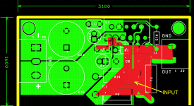
For DC (< 100 MHz), the current follows the path of least resistance. If you look at the image KSTR drew (Post #189) you'll see the forward current following the top layer traces and the return current returning directly from the speaker connector to the supply caps. That's the situation at DC.
Some people will argue over my definition of "RF" and "DC", but, seriously... Any frequency relevant to an LM3886 is DC as it behaves like DC. I consider frequencies up into the low 10s of MHz to be relevant for an LM3886.
Once the lengths of the PCB traces start approaching a significant fraction (5~10 % maybe) of the electrical(*) wavelength of the highest frequency of operation, I'd start considering using a more "RF" approach.
(*): The electrical wavelength is the wavelength measured on the board. I.e. the physical distance from voltage minimum to voltage minimum. They differ by a factor of the square root of the dielectric constant of the board dielectric.
~Tom
Just thinking of the magnetic forces between the supply and return currents in an almost zero ohm plane at any frequency. I am sure the return current doesn't follow the orderly path drawn by KSTR.
I did a sim in free tools for a really simple geometry
http://www.diyaudio.com/forums/loun...ch-preamplifier-part-ii-2373.html#post3049769
I really can't understand the 1 layer layouts for these power chip amps - even homebrew you can easily align masks to thru hole part tolerance, can solder pins both sides
http://www.diyaudio.com/forums/loun...ch-preamplifier-part-ii-2373.html#post3049769
so from 20 Hz to 2 kHz the inductance has dropped <20% due to gnd plane "current centroid" return path shifting towards the trace
by 20 kHz the effective loop area (~=inductance) has been reduced by <half due the proximity effect gnd plane current path crowding towards the trace
I really can't understand the 1 layer layouts for these power chip amps - even homebrew you can easily align masks to thru hole part tolerance, can solder pins both sides
Last edited:

Well... That's not how physics say the currents flow. First off, you need to think of it in terms of current density rather than as "lines of current". Secondly, current follows the path of least resistance. Your drawing of a magnetic field has more current (field lines) flowing along the longer paths.
I suggest you have a look at the tools JCX links to above.
~Tom
I suggest you have a look at the tools JCX links to above.
~Tom
It looks more like this for a simple point A to B flow. Red = high current density; blue = low.
~Tom
An externally hosted image should be here but it was not working when we last tested it.
~Tom
I don't believe currents flow in lines. I also don't believe currents leave the plane at the edges. Just an example of the spread of flow.
"current follows the path of least resistance" I have read this in several places put it cant be true, Current flows though all paths relative to the resistance. It does not only follow the path of least resistance.
My first example is somewhat exaggerating the spread of the flow and takes no consideration of the supply traces.
Last edited:
- Home
- Amplifiers
- Chip Amps
- LM3886 PCB vs Point-to-Point (with data)