Zobel at speaker cable side serves to different purpose - it terminates cable for HF at cable speaker end. Without that, the cable is driven from low amplifier output impedance and is open at speaker side, for HF. With Zobel added at cable speaker end the cable may be terminated for HF in some way, HF reflections are reduced and there is less HF interference on the cable. Same job is done with a resistor about say 200 ohm at cable speaker end, it absorbs some power, but is less inductive than Zobel capacitor. This works, and quite well. Remember I do not speak about Zobel added to amplifier output for stability purposes.
Back to the important question. I struggled to find anything on the output R-C compensation technique but this is a nice description of op-amp compensation techniques with the last method being the one.
http://www.st.com/st-web-ui/static/active/en/resource/technical/document/application_note/CD00176008.pdf
Note Figs 31 and 32
http://www.st.com/st-web-ui/static/active/en/resource/technical/document/application_note/CD00176008.pdf
Note Figs 31 and 32
In my view and experience, with chips amps the local output snubber does two main things, in order of importance :
- prevent/damp spurious oscillations of the output stage (way) above the closed-loop bandwidth by loading the output down. I'm completely with JohnW here. Chip amps typically have either quasi-complementary NPN output (LM3886) or a buffer with local feedback (TDA7293) for the negative half of output current swing and those are prone to oscillation. For that reason the snubber should go shortest path from output pin to the neg supply pin rather than ground and the decoupling at that frequencies should go rail-to-rail rathern than making a detour through ground.
- help phase margin by introducing a properly spaced pole-zero pair below closed-loop bandwidth, as given in consort_ee_um's link.
Back to the important question. I struggled to find anything on the output R-C compensation technique but this is a nice description of op-amp compensation techniques with the last method being the one.
http://www.st.com/st-web-ui/static/active/en/resource/technical/document/application_note/CD00176008.pdf
Note Figs 31 and 32
A lot of information not seen elsewhere.
I especially like the terminology used. Snubber network compensation, In-the-loop compensation and Out-of-the-loop compensation
I think I have been trying to promote "in the loop compensation" as the preferred method. Seeing Out-of-the-loop compensation as a crude band-aid.
Chip amps typically have either quasi-complementary NPN output (LM3886)
Yes, the are always HORRIBLE.
In my view and experience, with chips amps the local output snubber does two main things, in order of importance :
- prevent/damp spurious oscillations of the output stage (way) above the closed-loop bandwidth by loading the output down. I'm completely with JohnW here. Chip amps typically have either quasi-complementary NPN output (LM3886) or a buffer with local feedback (TDA7293) for the negative half of output current swing and those are prone to oscillation. For that reason the snubber should go shortest path from output pin to the neg supply pin rather than ground and the decoupling at that frequencies should go rail-to-rail rathern than making a detour through ground.
- help phase margin by introducing a properly spaced pole-zero pair below closed-loop bandwidth, as given in consort_ee_um's link.
Perhaps I should stick to the end of things I do know... Amplifiers and stability... 🙂
I do agree on the pole-zero pair formed by the Zobel network. This will help with stability if placed correctly. It also presents a load on the amp at HF, which is important for emitter follower output stages. Emitter followers tend to oscillate when operated with light load. This is a very common problem with beta-helpers in biasing circuits, actually.
The funny thing is that when I use a Zobel network and the output L||R network (I think some call this a Thiele network), the pole/zero of the Zobel seem to have no impact on loop gain/phase, hence, stability. I was using 700 nH || 10 R for the Thiele network. I haven't had time to drill fully into this, but I suspect the Thiele network ends up essentially separating Cload from the amp at frequencies relevant for stability. Perhaps I should do the mmm...mmmmath. Not a fan... 🙂
~Tom
PS: Thanks for the ST app note. That's good stuff.
I think I have been trying to promote "in the loop compensation" as the preferred method.
Even if you handled the compensation within the loop, you'd still need a circuit that applies a load to the output stage at HF.
The issue is that the ft roll-off of the output devices cause their output impedance to rise with frequency (i.e. become inductive). This sets up a resonant circuit with the parasitic caps and load caps in the system. This is a known issue with emitter followers and is not isolated to audio amplifiers. The solution to this is to ensure that the emitter follower output always sees a load. A simple resistor will do, but now you're burning DC power. Hence, the Zobel snubber circuit is actually a pretty elegant solution. There is no way to accomplish this in the loop as the loop has no gain at that frequency (I suppose you could have 1 ohm, 0.1 ohm in the feedback network, but I'm discarding that solution).
Driving capacitive loads is a challenge for any opamp. That's why there are book chapters and app notes written about it. It's also why you'll see some opamps marketed as "stable even with cap load". The traditional solution is to add some output impedance. A resistor in series with the output before the feedback tap point. That works well for low currents, but it'll kill your headroom (hence power specs) if you try that on an audio power amp. Isolating the load with a Thiele (L||R) network is a pretty elegant solution. Low tech. High reliability. Not broken...
~Tom
I can see we are not going to agree on this and I am sure we just have different approaches to the same problem.
I want to prevent the HF output. If the amp has no HF output there is no need to have a HF load.
I want to prevent the HF output. If the amp has no HF output there is no need to have a HF load.
Last edited:
The amp WILL have HF output if you leave its EF output floating at high frequency. This is called local oscillation. DWI! Deal... With... It... 🙂
~Tom
~Tom
There always is HF output -- it's called noise 🙂
The problem is when the output HF reaches the Negative input out of phase and completes the loop.
The amp WILL have HF output if you leave its EF output floating at high frequency. This is called local oscillation. DWI! Deal... With... It... 🙂
~Tom
I thought it worked something like this:
Oscilation is the signal re amplified over and over again though the feedback loop.
The zobel shorts the HF to ground preventing it from reaching the negative input.
The compensation capacitor in the feedback loop returns the HF signal in phase to the negative input preventing the oscillation.
Last edited:
Oh, I see what you're saying now. You're concerned that any HF present on the output will get back to the input and cause oscillations. That's not the case, because there's no loop gain available to make the amplitude grow. Even if the HF signal happens to arrive at the right phase on the inverting input, it does not see any gain. No oscillations start. The signal just gets attenuated by the amp.
Of course, this requires PM > 0, which is the case up to about 200 nF even without the Zobel network (see my simulations). You still need the Zobel network to provide a load for the amp at HF, though.
~Tom
Of course, this requires PM > 0, which is the case up to about 200 nF even without the Zobel network (see my simulations). You still need the Zobel network to provide a load for the amp at HF, though.
~Tom
Now we're cooking with gas!
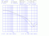
Then the moment we've all been waiting for LOOP GAIN measurements. In textbooks, the loop is opened and the gain "measured" or calculated. In practice this is not possible. However, by injecting a disturbance voltage into the feedback loop, the loop gain can be measured. This is documented well in an app note from HP: "Loop Gain Measurements with the HP 3577A Network Analyzer". Note that I did not bother to invert the phase, hence, the phase shown is actually the phase margin rather than the loop phase. Also note that the Tektronix CT-6 current transformer I'm using is intended for use at much higher frequencies. That causes the roll-off in the low end (<500 kHz).
The phase margin measures 68 º. The UGBW is 1.4 MHz. That's a bit higher UGBW than what I would have expected from the data sheet, but not completely out of whack. The PM is right on the money versus the data sheet specs.
The gain margin measures -14 dB. Not bad.
Gear: HP 3577A, Tektronix CT-6, HP 6237B lab supply, 8 Ω dummy load, Tektronix P6139 scope probes.
Supply voltage: +/-18 V.
Load: 8 Ω
Setup: LM3886 STAR GND P2P circuit.
~Tom
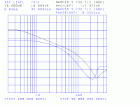
Attachments
Last edited:
Tom,
Brilliant work 🙂 really "Damn Good" 😀
I'm impressed - in fact I've got all excited and would like to try the same here - I've a 3577A in my basement somewhere and also a national instruments GPIB to USB pod (that will be harder to find in all my junk).
I've just ordered a HP "AC" Current probe so I can inject the signal into the UUT - like you my current probes I currently have to hand are all HF types, with limited LF B/W - although we don't really care about the LF is still nice to have as much LF BW extension as possible.
Couple of questions please if I may - How did you calibrate the system, I note the CT6 is not 1:1 "turns ratio" at 5mV per mA (not sure how / if this effects the results) - does the system monitor / normalize the injected signal to calibrate the resultant gain plot - (Am I correct to presume the "R" is a reference input after the injection point to allow normalization of the input signal gain to the UUT)?
Also how did you capture the data from your 3577A? presumably over GPIB - but is there a simple "Screen capture" software? Life is too short to install and then get to grips with the National Instruments software environment.
Can you offer any practical hints to getting the system going from your impressive efforts 🙂 for someone whose also going to try and setup the same system?
How many loops (turns) did you wrap around your current probe?
While I was messing with my "Discrete Component simulation circuit" of the LM3886 (which I could never get working correctly based on the published circuit so its results are somewhat dubious) - I noted that using 100nF / 10R Zobel network on the output resulted in peaking on the open loop gain plot at some point between 500kHz to 2MHz (forgive me, I don't recall the exact frequency). I had to reduce the "R" of the Zobel to say 3 Ohms to eliminate these peaks (a much lower R then one would normally expect to see in an ops Zobel) - and its interesting to note that NS/TI also use 2.7ohms on there App notes - so it gave some credence that my simulation model might be indicating a real effect - but I did not investigate further.
I'm wondering with your hardware measured Bode plot if you would also observe this peaking in the open loop response when when using a 100nF / 10R Zobel network?
Last edited:
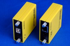
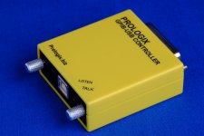
I use a Prologix GPIB-ETHERNET Controller to control my test equipment and to get the screen captures. John Miles has an excellent toolkit for the Prologix controllers including a plotter emulator.
I've used the GPIB-USB version as well. It works just as well you just have to connect via USB rather than ethernet. I find the ethernet version to be more of a "set and forget" solution as it's always plugged into my network. I have the USB version for sale ($120), just PM me if you're interested.
The CT-6 current probe only takes one turn, or rather half a turn. I threaded the pin of the feedback resistor through the current probe. So LM3886 output -> CT-6 -> FB resistor.
I calibrated the system by placing both probes on the feedback resistor side of the current probe, performing a sweep (1 Hz RBW, 5 sec, log), and hitting Normalize in the calibration menu. Then the A Channel probe was moved to the amp output. The Ref Channel stayed on the feedback resistor side.
~Tom
Attachments
If your using the Current Probe method to inject the stimulus signal into the loop - the HP Application note states:-
“In order to work properly, the Probe must be used at a point where the Driving impedance (I read this to mean the current Probes "Output Impedance") is quite low compared to the load impedance (Which I understand to be referring to the impedance of the circuit node at the stimulus signal injection point).”
Also:-
“The efficiency of this current injection scheme is generally poor. In order to couple enough signal into the loop for an adequate S/N ratio, it maybe necessary to pass the pickup wire (Node) through the current probes cavity several times.”
With the LM3886 being an "integrated device" you don't have the option to access the internal high impedance VAS to OPS signal node (or any other high impedance Node) - so your forced to inject the stimulus signal "against" the output stages "native" output impedance. The fact that you have achieved the measured results only goes to confirm how poor the LM3886 open loop output impedance is - certainly at increasing Freq.
I was at first surprised at how low the indicated LF gain was on your Bode Plots, but upon reflection you are not only battling against the CT-6 LF B/W limitations but also at the same time working against OPS decreasing OPS impedance towards DC – both these effects will impact the LF portion of the Bode plots.
At least the Loop Gain plots appears to indicated the main area of concern 🙂
Thank you for your offer of the Prologix GBIP to USB – Seems like they have become far more professional – I remember when they where just bare PCB with Heatshrink wrap.
I should have a NI GPIB to USB controller which I was using with John Mile’s Screen capture software with my HP3585A – must have had a brain fart as for some reason I thought it was just for the 3585A. If I cannot find my USB controller or have problems getting it going once again – than I’ll be more then happy to purchase your Prologix unit – thank you.
I last visited Johns Site maybe 4 years ago – wow its nice to see how its developed since 🙂 Some really useful software nuggets – and much expanded device support with the latest Software 🙂
Again - well done in getting real world loop gain measurements 🙂
If your using the Current Probe method to inject the stimulus signal into the loop - the HP Application note states:-
“In order to work properly, the Probe must be used at a point where the Driving impedance (I read this to mean the current Probes "Output Impedance") is quite low compared to the load impedance
Finding a good spot to break the loop is always a challenge.
“The efficiency of this current injection scheme is generally poor. In order to couple enough signal into the loop for an adequate S/N ratio, it maybe necessary to pass the pickup wire (Node) through the current probes cavity several times.”
That's probably true for a current probe intended for measuring several Ampere. The CT-6 gain is 5 mV/mA and is intended for low current use. Its cavity is only a bit over 1 mm in diameter, so feeding the wire through twice is not an option.
I was at first surprised at how low the indicated LF gain was on your Bode Plots, but upon reflection you are not only battling against the CT-6 LF B/W limitations but also at the same time working against OPS decreasing OPS impedance towards DC – both these effects will impact the LF portion of the Bode plots.
Yep. As you can see from the slope in the 400 kHz - 4 MHz region, it's a -20 dB/dec slope. Just as you'd expect. I think it's fair to extend that towards the LF region.
At least the Loop Gain plots appears to indicated the main area of concern 🙂
Which was the point... 🙂
Thank you for your offer of the Prologix GBIP to USB – Seems like they have become far more professional – I remember when they where just bare PCB with Heatshrink wrap.
Dang! He really hit jackpot with that controller. Open source software. Easy to interface to. Less that half the price of the NI controllers that require proprietary software. You can get them through various distributors now as well.
Again - well done in getting real world loop gain measurements 🙂
Thanks! Next step will be to build the op-amp summer mentioned in the HP app note. That should extend the LF coverage.
~Tom
Last edited:
- Home
- Amplifiers
- Chip Amps
- LM3886 PCB vs Point-to-Point (with data)