Ah in that case I'd suspect input LTP RF sensitivity as the cause of HF hash.
I am using RC filter on the LTP input.
Yesterday, I listened my version of VSSA. I improved the CCS and used low Cob transistor on VAS. I notice the different on high frequency, it is subtle change but better. I do not know the reason of this, may be the better CCS or VAS transistor or both.
I am using RC filter on the LTP input.
Suggest trying an LC filter - RC being single pole isn't really steep enough. Normally only around -20dB by 2MHz. Also check that the 'C' to ground in your filter isn't to the input gnd, this is normally contaminated by CM noise.
Last edited:
Bimo are you saying that total configuration sounds bad or each of those "features" sounds bad in your experience?
Obviously 99% of CFA designs are symmetrical and a lot use Cascode VAS etc.
No. I am not compare to the topology of VFA and "CFA". I have design my VFA long years ago. I measured the THD at that time and it is slightly better than the simulating VSSA which is "CFA". My VSSA is slightly different than LC's VSSA or Shaan's PeeCeeBee, because I am using parts that available here.
I want to know what was make the sound different.
My goal is how to make better design, with VFA or "CFA".
Suggest trying an LC filter - RC being single pole isn't really steep enough. Normally only around -20dB by 2MHz. Also check that the 'C' to ground in your filter isn't to the input gnd, this is normally contaminated by CM noise.
Thank you for your suggestion about LC filter.
I always using 10 Ohm resistor to connect "clean" ground and "dirty" ground from 14 years ago 😀 for audio amplifier. Implementation of good ground and components layout is a must. At that time I was video engineer. Bad layout (including PCB track) can degrade tuner performance and reduce S/N ratio in audio circuit.
RF beads can work work wonders as well. Make sure the ground side of your input socket is connected right at the chassis next to it with a 500 pF to 1 nF cap.
Kgrlee showed a very nice diagram on this thread a while back that addressed this very point.
Kgrlee showed a very nice diagram on this thread a while back that addressed this very point.
RF beads can work work wonders as well. Make sure the ground side of your input socket is connected right at the chassis next to it with a 500 pF to 1 nF cap.
Kgrlee showed a very nice diagram on this thread a while back that addressed this very point.
I used Ferrite beads to connect analog ground and digital ground on my video tape recorder design. But it is difficult to get Ferrite beads on local market here.
Made PCB for DIY is relative easy than for mass product. Usually, in mass product, the casing and all mechanics is designed first then followed by PCB design and many trade-off made here.
Last edited:
cascodes
BTW, with unmatched PNP-NPN trannies, it is still possible to minimize the 3rd harmonic. However, due to the asymmetry, the 2nd harmonic which will be much larger.

Nope! Depending on the kind of compensation (ordinary Miller, shunt or MIC) it is of the order between +/0.5mV and +/-5mV (just sim it).[..]
Further, in #3135 you claim that Cob effect cancellation requires constant Vce. That is incorrect, it requires constant Vcb. Though I would agree that your cascode common emitter is theoretically better in cancelling the Cob. In your case, the Vcb variation is defined by the variation of a practical ~1.3V voltage source (like two forward biased diodes) with the current ( say +/-50mV),
Nope! That would make about <0.4% for mine vs. 7% yours.while mine keeps Vcb at the reference voltage (say 15V) +/- the input signal (say +/1V). That would make about 4% for yours vs. 7% mine. [..]
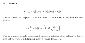
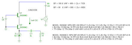
I disagree. Although the output impedance (ro) of a common emitter bjt is determined by the Early voltage (VA) and Ic of course, it's a different story in case of a common base bjt. Now the output impedance (of the output bjt) is largely determined by VA and beta as well (see Feucht, 1st pic). As you know, see your own comment, for a given manufacturing process, the product: VA * beta is roughly constant. So increasing VA is of no use, as at the same time beta will decrease. As a result, the output impedance doesn't rise at all. Even worse, a higher Early voltage is counterproductive! I've simmed a cascode with several trannies and in every case the output impedance decreased somewhat after doubling VAF and halving BF (see 2nd pic).Regarding the common base stage of the cascode, I could be missing something, but IMO a high Early voltage device is mandatory. Otherwise, the common base device would be subject to the same Early effect that the cascaded common emitter device is. What I'm saying is that e.g. cascoding two identical devices doesn't make much sense.
I'm afraid I have to agree with that. Nevertheless, I think that people should be aware of the (theoretical) possibilities of minimizing distortion and cancellation of 'disturbances' from the current sources.Finally, I think what you are proposing here is essentially an intellectual game. You mentioned yourself that this works only with perfectly matched transistors (modeled here as ideal CCCS), and temperature compensation is not yet considered. This, and the fact that I would not expect anyway to have the IPS dominate the distortions in the global picture, IMO makes this setup of little practical interest.
BTW, with unmatched PNP-NPN trannies, it is still possible to minimize the 3rd harmonic. However, due to the asymmetry, the 2nd harmonic which will be much larger.
You are still on my ignore list, but it is totally ineffective when you are cited by other members.P.P.S. I thought I'm on your ignore list, but I see you are following me pretty close?!
Attachments
Nope! Depending on the kind of compensation (ordinary Miller, shunt or MIC) it is of the order between +/0.5mV and +/-5mV (just sim it). <...> Nope! That would make about <0.4% for mine vs. 7% yours.
Perhaps, I will take a closer look when I'll find some time but, 0.4% or 7%, still to small to make any measurable difference. To add insult to injury, the Cob vs. Vcb curve derivative around 1V is much larger than around 15V, so I would expect those 0.4% to have a much larger effect in modulating Cob than what you would think, by comparing two percentages only.
For the rest, I've already thanked Marcel for the heads up.
You are still on my ignore list, but it is totally ineffective when you are cited by other members.
I'm so sorry to hear this, can I do something to help?
Perhaps YOU can explain to me why it is OK to operate with a ULGF greater than the OPS pole with a CFA, while it is not OK to do it with adequate margin with a VFA.
Cheers,
Bob
Bob the answer is speculative but seems only Self, who also deems CFA amps rubbish has some theory about it, although he mentions in his book that more study is required. His insight is with VFA but if one looks closer its obvious why this is a factor in CFA. At the start of this thread I mentioned that Triple EF stages seem to be taylor made for CFA amps where stability is concerned and many ridiculed this.
The answer can be found in Selfs book, the part to study is regarding the shunt compensation cap to ground and the effect it has on the outputstage. Although other compensation methods have been shown here, its shunt compensation that best works on CFA. I wont speculate whether their use has the same effect as the traditional shunt compensation that usually applies to CFAs.
Although other compensation methods have been shown here, its shunt compensation that best works on CFA
There is absolutely no technical reason that would make this statement true, and repeating it also doesn't help.
Shunt lag compensation is probably the worst compensation method. To quote Peter Baxandall "The technique is in all respects sub-optimal". D. Self discusses this at large, and if I recall correctly so does Mr. Cordell, in their books. If you have any arguments as of why shunt lag compensation is preferred for "CFA"s please present your technical arguments.
The only case in which a lead-lag shunt compensation can be really useful is to compensate the Miller loop.
Hi Bonsai,
If I am not mistaken, here you have succinctly stated why the CFP is distinguished from a VFA insofar as amount of feedback that can be used to reduce distortion. (Sometimes I am a slow learner).
So the suggestion is that the CFA topology allows us to operate at ULGF above the OPS pole, while the VFA generally does not (perhaps with the caveat that it is true for a given level of complexity of the compensation). Is this a fair way to put it?
I somehow think it is dangerous to operate ULGF above the OPS pole for any amplifier, and my knee-jerk reaction is that I can make a VFA operate with a ULGF above the OPS pole by as much as a CFA with the same level of risk with proper design of the VFA targeted to that goal. Am I wrong? Maybe I just don't understand the silver bullet of CFA that permits one to do better in regard to operating ULGF above the OPS pole.
I think we all agree that in reality there is more than one OPS pole and that it can move around quite a bit with output current, output voltage and output load. That is why I am so distrustful of it.
Cheers,
Bob
Bob, I don't think the ULGF should be above the OPS pole so we are in agreement.
I am simply saying that the lower OLG on CFA's means less of the phase shift at HF is exposed before the typical ULGF of VFA's. (Note I am not saying that high gain= phase shift)
I think this explains why CFA is more tolerant of cap loads, and they are easier to comp.
Again, I am not dissing VFA - I've built and listen to both types. 😎
There is absolutely no technical reason that would make this statement true, and repeating it also doesn't help.
Shunt lag compensation is probably the worst compensation method. To quote Peter Baxandall "The technique is in all respects sub-optimal". D. Self discusses this at large, and if I recall correctly so does Mr. Cordell, in their books. If you have any arguments as of why shunt lag compensation is preferred for "CFA"s please present your technical arguments.
The only case in which a lead-lag shunt compensation can be really useful is to compensate the Miller loop.
Waly, really ???, Im going to follow Edmonds example and just put you on the ignore list.
Please note I said nothing about shunt being a good compensation method for voltage feedback amps. A couple of weeks ago you said my exact same words, Shunt is best for CFA, now you changed your mind again. So now which is it ? Before that you argued high and low that diamond buffer is not more linear than a LTP then to 3 weeks later state that it is, obviously you went to consult your books. Do you have to do this everytime ?
A couple of weeks ago you said my exact same words, Shunt is best for CFA
- Please quote me, I don't recall saying that shunt compensation is good for CFAs.
- Please present your arguments as of why shunt compensation is optimal for CFAs.
- Then please put me on your ignore list. I would be proud to get a place there.
Here you go:- Please quote me, I don't recall saying that shunt compensation is good for CFAs.
Shunt compensated CFAs excel at all these attributes, they simply can't be beaten by any other topology.
- Please quote me, I don't recall saying that shunt compensation is good for CFAs.
- Please present your arguments as of why shunt compensation is optimal for CFAs.
- Then please put me on your ignore list. I would be proud to get a place there.
Sorry I have better things to do than waste any more of my precious time on your ramblings. If you dont recall nonsense you said before you ran off to consult your books and get the right answers, buy a recorder from wallmart.
Sorry I have better things to do than waste any more of my precious time on your ramblings. If you dont recall nonsense you said before you ran off to consult your books and get the right answers, buy a recorder from wallmart.
Manso, I must say that Waly contribution to this thread is apreciated by me, and I hope by others, his knowledge is quite high and helps my rusty brain to think again about what I learned at University, and he just began to acknowledge some of his mistake, don't discourage him.
Damir
He only said: "a common-emitter stage with cascode on top still has a much higher output resistance than a plain common-emitter stage"[..]
For the rest, I've already thanked Marcel for the heads up.
That's not equivalent to what I just posted, where I made clear that a so called 'mandatory' high Early voltage bjt is pointless and probably even counterproductive.
Sure, just be nice, polite en cooperative.(regarding ignore list)
I'm so sorry to hear this, can I do something to help?
Cheers, Edmond.
Have you started the year with the firm resolution to believe in Santa Claus?Sure, just be nice, polite en cooperative.
Btw: Thanks for so many clever and useful analyses you bought to the community, Ed.
I'll just throw up some sources from time to time. Bob, Dave, etal let me know if you found your answer in one of these: If not, I'll keep trying --
www.ieee.li/pdf/viewgraphs/current_feedback_vs_voltage_feedback_amplifiers.pdf
www.dspace.thapar.edu/dspace/bitstream/10266/1306/3/1306.pdf
Thx-RNMarsh
View attachment op-amp-cf-sloa080.pdf
-RNMarsh

- Home
- Amplifiers
- Solid State
- CFA Topology Audio Amplifiers