R6 is to linearize the bias spreader over a wider temperature range.
Over wider VAS/TIS current fluctuation!
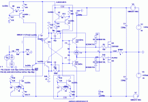
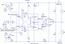
As promised here is the simple concept CFA - again, let me stress this is just an idea to show that you can ditch the feedback capacitors. What we in fact are doing here is moving them from the feedback network to the input coupling. Total of 6 active devices. If its packages you really want to reduce, replace the front end transistors with a dual N/P SMD device (NXP, Diodes Inc, Rohm et al) and you will get better thermal drift performance as well.
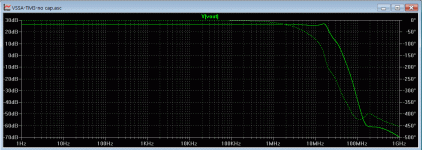
As you can see the bandwidth is extremely wide at ~10 MHz and the slew rate also very high. Distortion is about 0.02% at 40W output at 20 kHz
I have one in the back of my head that uses 2 mosfets in the output stage, and a dual N/P packagage input stage . . . . so 4 active devices in total 3 packages. Distortion of course about 20 dB higher.
😎
Attachments
Last edited:
As promised here is the simple concept CFA - again, let me stress this is just an idea to show that you can ditch the feedback capacitors. What we in fact are doing here is moving them from the feedback network to the input coupling. Total of 6 active devices. If its packages you really want to reduce, replace the front end transistors with a dual N/P SMD device (NXP, Diodes Inc, Rohm et al) and you will get better thermal drift performance as well.
As you can see the bandwidth is extremely wide at ~10 MHz and the slew rate also very high. Distortion is about 0.02% at 40W output at 20 kHz
I have one in the back of my head that uses 2 mosfets in the output stage, and a dual N/P packagage input stage . . . . so 4 active devices in total 3 packages. Distortion of course about 20 dB higher.
😎
Almost like VSSA.... you eliminate feedback capacitors.
As promised here is the simple concept CFA - again, let me stress this is just an idea to show that you can ditch the feedback capacitors. What we in fact are doing here is moving them from the feedback network to the input coupling. Total of 6 active devices. If its packages you really want to reduce, replace the front end transistors with a dual N/P SMD device (NXP, Diodes Inc, Rohm et al) and you will get better thermal drift performance as well.
As you can see the bandwidth is extremely wide at ~10 MHz and the slew rate also very high. Distortion is about 0.02% at 40W output at 20 kHz
I have one in the back of my head that uses 2 mosfets in the output stage, and a dual N/P packagage input stage . . . . so 4 active devices in total 3 packages. Distortion of course about 20 dB higher.
😎
One of the attractions of VSSA is that it is DC coupled and the output offset is easily adjustable. Some of the work I do with speakers is to add a DC offset from the preamp side and measure distortion versus DC offset.
I suspect that eliminating the DC coupling will be a non-starter for other VSSA followers.
This, and the high distortion (0.02%).I suspect that eliminating the DC coupling will be a non-starter for other VSSA followers.
Bonsai, i believe the points were feedback is kept is bad: it destroy damping factor, and can increase distortion a lot. Feedback has to be taken at the exact speakers output point. Even a little unbalance in high current tracks can increase HD by an order of magnitude (tested since 1970 🙂.
As promised here is the simple concept CFA - again, let me stress this is just an idea to show that you can ditch the feedback capacitors. What we in fact are doing here is moving them from the feedback network to the input coupling. Total of 6 active devices. If its packages you really want to reduce, replace the front end transistors with a dual N/P SMD device (NXP, Diodes Inc, Rohm et al) and you will get better thermal drift performance as well.
As you can see the bandwidth is extremely wide at ~10 MHz and the slew rate also very high. Distortion is about 0.02% at 40W output at 20 kHz
I have one in the back of my head that uses 2 mosfets in the output stage, and a dual N/P packagage input stage . . . . so 4 active devices in total 3 packages. Distortion of course about 20 dB higher.
😎
Looks like an old elektor igbt amp design. But nice.. No doubt
Same problem..... since forever.... and others here --> do not bias via the base of Q1 and Q2. Bias the Q1,2 via each emitter and then can take input direct to bases and eliminate C1 and C2. As a suggestion, only, of course.
But as is -- what affect on THD would bypassing D1-4 with large value C and/or increasing R17-18 value.
Thx-RNMarsh
But as is -- what affect on THD would bypassing D1-4 with large value C and/or increasing R17-18 value.
Thx-RNMarsh
Last edited:
I propose this (very simple VSSA like, but without evil Caps).
The first emitter follower is not included in the loop, to don't add a pole.
It is damn damn fast. (1400V/µs ?)
HD 1KHz 50W = 0.000583%
HD 20KHz 50W = 0.002736%
Replacing the second stage CCSs with simple 470 Ohms resistances still reduce 20 kHZdistortion. 0.002410 at 20kHz while it increase 1kHz to 0.000623%.
Attachments
Last edited:
It gives this.
HD 1KHz: 0.000327%
HD 20KHz: 0.002299%
Better than expected once offset tuned.
Note:i had let the double feedback path, but it is a single one, now (shorted). Better for distortion when resistances are not the exact same values.
HD 1KHz: 0.000327%
HD 20KHz: 0.002299%
Better than expected once offset tuned.
Note:i had let the double feedback path, but it is a single one, now (shorted). Better for distortion when resistances are not the exact same values.
Attachments
Last edited:
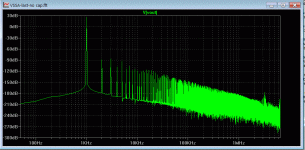
3rd, 5th 7th etc are bigger than even harmonics.
Some of this Forum have very strong opinions on what that does to the sound, even though the levels look VERY LOW @ <-110dB.
Some of this Forum have very strong opinions on what that does to the sound, even though the levels look VERY LOW @ <-110dB.
It gives this.
HD 1KHz: 0.000327%
HD 20KHz: 0.002299%
Better than expected once offset tuned.
Note:i had let the double feedback path, but it is a single one, now (shorted). Better for distortion when resistances are not the exact same values.
Acording to LC, diamond buffer on input sound worse. Of course it is not about THD, at least in simulation. I want to know why?
I modified Bonsai's schematic. (Don't laugh!). I think it is OK, using cap on input. But I do not know about DC offset stability and if this compensation is correct or not.
Attachments
Dear Esperado
I checked your VSSA in MC9.
Without the emitter resistors in the circuit diagram of the input transistors is not workable.
But even with the emitter resistors 47 ohm and current output transistors 300 mA distortion at 1 kHz with an output voltage of 25 V (peak) is equal to 0.3% into 8 ohms
best regards
Petr
Petr1951, i don't understand: What the hell ?
What happens with simulators, or at least LTPspice ? Is- it anything we can rely on ?
I begin to just hate those programs, so badly coded, with a so unfriendly user interfaces, incomplete GUI, no serious debug help etc.
Anyway, it is not my way to design: Schematic, calcul, build, modify and listen, listen listen.
So, if any problem with my file (attached) please, can-you explain ?
The currents in this sim are: 1.7mA in the input stage, 1.4mA in the second, 5mA in the driver (not enough), 150mA in the OPS.
Attachments
Last edited:
That is my experience too. May-be it is a question of stability at the very sensible point where feedback is abstracted from the signal (input transistor).Acording to LC, diamond buffer on input sound worse. Of course it is not about THD, at least in simulation. I want to know why?
In this matter, it is very subjective on my side: made several attempts, was always disappointed, took it for granted. Not very scientific ;-).
Dear Esperado
I have several years working with MC9 and trust this program . Prior to that used Multisim .
Yeah, I got a collector current of 1.7 mA input transistors
but the current of the second transistor is only 0.6 mA
and this current is not enough to open the transistor voltage amplifier (VAS) .
When I added the resistors in the emitter circuit current of the input transistors of the second transistor current mirror according to the law was equal to the current input transistors .
The disadvantage of a voltage amplifier (VAS) is also a lack of emitter resistors. In schemes were VSSA 10 ohms. I think that without them is a low thermal stability . I modeled without these resistors.
When I reduced the quiescent current of the output transistors to the optimum for class AB , that is, up to 120 mA of distortion increased to 1%
regards
Petr
I cannot understand those huge differences between You and I.but the current of the second transistor is only 0.6 mA.
Models ?
One thing is boring, here, it is that the emitter resistance of the second input stage is both part off the feedback network, and bias.
So, if you want to increase the feedback impedance value to set higher stability margin, you have to change the emiter resistance value too (and collector accordingly). With a big impact on its bias and distortion.
Agree, since the most important, the OPS bias is set independently by V10. Anyway, i believe a full DC coupled amp cannot work properly without a servo regarding offset thermal stability.The disadvantage of a voltage amplifier (VAS) is also a lack of emitter resistors. In schemes were VSSA 10 ohms. I think that without them is a low thermal stability .
From post http://www.diyaudio.com/forums/solid-state/240712-cfa-topology-audio-amplifiers-83.html#post3671842 :
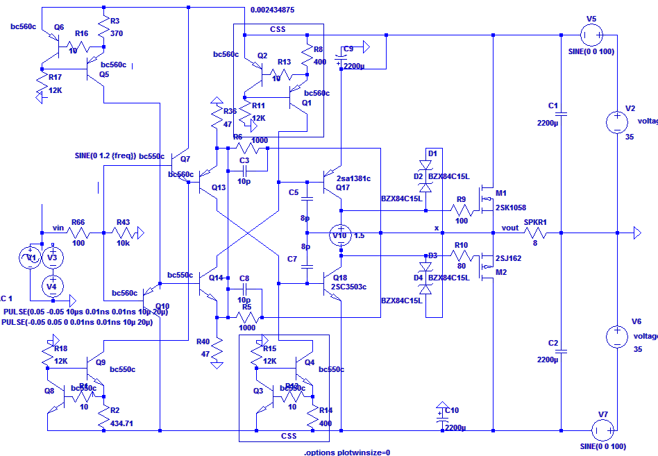
For me, a quite puzzling schematics :
R36 // R40, R5 // R6, C3 // C8
Why paralleling components ?
Voltages around the CCS (positive branch) :
emitter of Q17 at +35 V => base of Q17 at +35V - (1*Vbe)
emitter of Q2 at +35 V => base of Q2 at +35V - (1*Vbe)
emitter of Q1 almost equal to base of Q2 => base of Q1 at +35 - (2*Vbe)
Is the CCS works as intended if the voltage at collector of Q1, which is connected to base of Q17, is almost equal to the voltage at its emitter ?
The schematics of the following post has got rid of the CCSs.
- Home
- Amplifiers
- Solid State
- CFA Topology Audio Amplifiers