Train just bunched up on me. Could you explain further. What do you mean, high output?
If you want to increase the power output of an amplifier design, given the same (nominally) resistive load, then both the voltage and the current requirements increase. Each output FET must operate within its safe operating area (SOA) which is usually defined by a region in voltage-current space.
A typical way to design high power amplifiers is to parallel many output FETs, dividing the current between them. A major disadvantage with paralleling N FETs is the gate capacitance is multiplied by N. (BTW: Balanced amplifiers have an advantage of dividing the output FET voltage requirements by a factor of 2, for the same output power).
The cascoded design I presented has for each rail a single FET (FETcs) in common source mode driving multiple paralleled FETs (FETcg) in common gate mode (ie. the cascode FETS). The drain-source voltage on FETcs is kept low (and constant) but its drain current is quite high, but within its SOA. The drain-source voltage on cascode FETcg is quite high, but the drain current is 1/N the drain current of FETcs, again with its SOA.
BTW: Most high power amplifiers that I am familiar with run the output FETs in common-drain (source-follower) mode rather than common source. This still requires driving a high gate capacitance of paralled FETs, but due to bootstrapping only the gate-to-drain capacitance is important. Also such amplifiers usually require at lease 3 stages, an additional intermediate stage being required to generate the high voltage swing to drive the source-follower output stage.
Last edited:
Ok you got us (well me at least) - what's the downside then ? Reduced voltage swing at the outputs for a given rail voltage vs non cascodes?
Ok you got us (well me at least) - what's the downside then ? Reduced voltage swing at the outputs for a given rail voltage vs non cascodes?
Yes, some voltage swing is a sacrificed due to cascoding, which means somewhat higher idle power dissipation for the class-A output power.
Cascoding is not the magic solution for everything.
Apart from some people suggesting that they do not always sound better,
there is interaction between the cascode device and the gain device at high frequencies.
In many cases, you can see this as overshoot with a 10kHz square wave.
No free lunch.
Patrick
Apart from some people suggesting that they do not always sound better,
there is interaction between the cascode device and the gain device at high frequencies.
In many cases, you can see this as overshoot with a 10kHz square wave.
No free lunch.
Patrick
This is certainly intriguing - i am not so much (yet) a fan of balanced f5 only because I don't think i have exhausted the possibilities from 2 stage amps.
Once I have, then I can move on ambitiously to 4 stage amps that these balanced designs represent. You all probably have been down the same path so likely, will I.
These cascodes seem like a different kettle of fish altogether. Anyway will watch (as chancellor palpatine one said) with great interest.....
If you want to increase the power output of an amplifier design, given the same (nominally) resistive load, then both the voltage and the current requirements increase. Each output FET must operate within its safe operating area (SOA) which is usually defined by a region in voltage-current space.
A typical way to design high power amplifiers is to parallel many output FETs, dividing the current between them. A major disadvantage with paralleling N FETs is the gate capacitance is multiplied by N. (BTW: Balanced amplifiers have an advantage of dividing the output FET voltage requirements by a factor of 2, for the same output power).
The cascoded design I presented has for each rail a single FET (FETcs) in common source mode driving multiple paralleled FETs (FETcg) in common gate mode (ie. the cascode FETS). The drain-source voltage on FETcs is kept low (and constant) but its drain current is quite high, but within its SOA. The drain-source voltage on cascode FETcg is quite high, but the drain current is 1/N the drain current of FETcs, again with its SOA.
BTW: Most high power amplifiers that I am familiar with run the output FETs in common-drain (source-follower) mode rather than common source. This still requires driving a high gate capacitance of paralled FETs, but due to bootstrapping only the gate-to-drain capacitance is important. Also such amplifiers usually require at lease 3 stages, an additional intermediate stage being required to generate the high voltage swing to drive the source-follower output stage.
Why multiple cascodes? How high are you taking voltage to overcome voltage swing limitation imposed by topology. While you reduce the voltage the main fet sees, you have to significantly increase the currennt to make up for the fact that it stands alon in its duties. Also, when paralleling fets, isnt it tru that Yfs increases as well, reducing some of the miller C that results. As you say, Nelson uses source followers with capable Vas stages.
Cascoding is not the magic solution for everything.
Apart from some people suggesting that they do not always sound better,
there is interaction between the cascode device and the gain device at high frequencies.
In many cases, you can see this as overshoot with a 10kHz square wave.
No free lunch.
Patrick
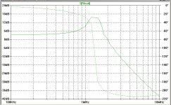
An unexpected 1.5 MHz high frequency resonance (shown below) appeared in the AC analysis of my cascoded balanced F5 design but not in the cascoded circlotron. This is in designs with no inductors and no capacitors other than those associated with the JFETs and MOSFETs.
Since I haven't yet built this design, I do not know what surprises await. I know that Spice simulation is often inadequate, mostly due to poor device models for the active devices.
BTW: Does anyone know how fast MOSFET thermal runaway occurs? Without source degeneration resistors this issue worries me, and I suspect that a current servo would be too slow to respond. How about appropriate MOSFETs with a positive temperature coefficient?
Attachments
Last edited:
An unexpected 1.5 MHz high frequency resonance (shown below) appeared in the AC analysis of my cascoded balanced F5 design but not in the cascoded circlotron. This is in designs with no inductors and no capacitors other than those associated with the JFETs and MOSFETs.
Since I haven't yet built this design, I do not know what surprises await. I know that Spice simulation is often inadequate, mostly due to poor device models for the active devices.
BTW: Does anyone know how fast MOSFET thermal runaway occurs? Without source degeneration resistors this issue worries me, and I suspect that a current servo would be too slow to respond. How about appropriate MOSFETs with a positive temperature coefficient?
I almost said something about this, but servos are a new game(like everything else) and I just didnt know. Controlling offset seems to be a slower process than thermal runway.
Why multiple cascodes? How high are you taking voltage to overcome voltage swing limitation imposed by topology. While you reduce the voltage the main fet sees, you have to significantly increase the currennt to make up for the fact that it stands alon in its duties. Also, when paralleling fets, isnt it tru that Yfs increases as well, reducing some of the miller C that results. As you say, Nelson uses source followers with capable Vas stages.
Not multiple cascodes in series, just in parallel as shown in post #96 http://www.diyaudio.com/forums/pass-labs/213152-balanced-f5-small-footprint-10.html#post3456193.
Mind showing example of voltages and currents. How high do you intend to take the current for the drive fet and what voltage will it see at its drain. Isnt this ultimately what limits the power(current) swing(voltage) of the stage?
f5 is already high bandwidth amp, so no degeneration is the main change. I dont know that the Cascode does anything for that.
f5 is already high bandwidth amp, so no degeneration is the main change. I dont know that the Cascode does anything for that.
Lhquam, if you have time, maybe take us down the spice road ? Simple sim (with values not params so we can get our heads round this ) of a basic f5 or f6 with models and an asc file and then again with cascodes. I find it (and perhaps i am the only one) a little tough to follow your sims mentioned above
Mind showing example of voltages and currents. How high do you intend to take the current for the drive fet and what voltage will it see at its drain. Isnt this ultimately what limits the power(current) swing(voltage) of the stage?
f5 is already high bandwidth amp, so no degeneration is the main change. I dont know that the Cascode does anything for that.
I do not intend to build such a big amp, but here is a hypothetical amp.
Unbalanced F5 cascode topology
- 400 W Class-A output
- 86 volt rails
- 5A idle current
- 6 volt cascode voltage (Vds of FETcs)
- common source FET dissipates 6V * 5A = 30 watts
- cascode FETs dissipate a total of 80V * 5A = 400W
- with 12 cascode FETs per rail, each FET dissipates 33.3W
A better approach would be:
Balanced F5 cascode topology
- 400 W Class-A output
- 46 volt rails
- 5A idle current
- 6 volt cascode voltage (Vds of FETcs)
- common source FET dissipates 6V * 5A = 30 watts
- cascode FETs dissipate a total of 40V * 5A = 200W
- with 6 cascode FETs per rail, each FET dissipates 33.3W
Lhquam, if you have time, maybe take us down the spice road ? Simple sim (with values not params so we can get our heads round this ) of a basic f5 or f6 with models and an asc file and then again with cascodes. I find it (and perhaps i am the only one) a little tough to follow your sims mentioned above
I first used Spice in about 1983, and I only recently (3 years ago) resumed using LTSpice. I am still learning about its tricks and limitations. It would be an enormous undertaking to do a complete job of this for the entire amplifier. Something like a multi-week college course. I am not sure where to start.
help the much less skilled...
I am in the pursuit of building a F5. Was going down the F5T path, but got stopped when I started reading about the Balanced F5 here.
At this moment if it weren't for recent posts here) I would be headed down the lhquam Balanced F5 path.
However, I was also stuck trying to figure out how to use my 40-0-40 480VA xformer which was going to give me too high of rails or require a choke in the PS. I hate accumulating parts - I have too many "some day" parts - so was really trying to figure out how use tranny.
So my question. Will this latest design discussion allow higher rails and result in something I can use my PS xformer in or should I quickly get on the buzzforb GB (if I still can)? Or still wiser to wait for this discussion to settle?
I first used Spice in about 1983, and I only recently (3 years ago) resumed using LTSpice. I am still learning about its tricks and limitations. It would be an enormous undertaking to do a complete job of this for the entire amplifier. Something like a multi-week college course. I am not sure where to start.
Actually what I meant was a simple demo of the f5 cascode topology in an asc file so that anyone with ltspice can run and compare with non cascode f5. If you can specify values for the components and models for the actives that would be nice so we are all on the same page. Thank you.
Actually what I meant was a simple demo of the f5 cascode topology in an asc file so that anyone with ltspice can run and compare with non cascode f5. If you can specify values for the components and models for the actives that would be nice so we are all on the same page. Thank you.
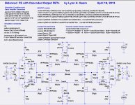
That I can do. I will clean up the balanced, cascoded F5 .asc file and post it.
In my present .asc file, most of the component values are parameterized because they depend on many design choices such as bias current, MOSFET parameters, etc. Some parameters might not need to be parameterized, but sometimes it is convenient to use the Spice .step command to explore the effect of changing some of these parameters. Thus I am reluctant to strip out the parameterization.
How will the fets perform with only 6V on the drain. Even with high current, that is putting them in interesting territory. do you have distortion numbers to look at
How will the fets perform with only 6V on the drain. Even with high current, that is putting them in interesting territory. do you have distortion numbers to look at
Which power level are you talking about. The high power (400W) amplifier with the IRFP240/9240 or FQA28N15/36P15 might not do well at 6V Vds and 5A-10A Id. That design was a response to your query and I haven't really flushed out the design issues. A higher cascode voltage is probably needed, resulting in higher power dissipation in the common-source FET.
However, at the 40W-50W power level of "Balanced F5 in a Small Footprint",
looking at the datasheets, those FETs appear to be running in a good I-V region.
Actually what I meant was a simple demo of the f5 cascode topology in an asc file so that anyone with ltspice can run and compare with non cascode f5. If you can specify values for the components and models for the actives that would be nice so we are all on the same page. Thank you.
Here it is!

Attachments
Last edited:
Which power level are you talking about. The high power (400W) amplifier with the IRFP240/9240 or FQA28N15/36P15 might not do well at 6V Vds and 5A-10A Id. That design was a response to your query and I haven't really flushed out the design issues. A higher cascode voltage is probably needed, resulting in higher power dissipation in the common-source FET.
However, at the 40W-50W power level of "Balanced F5 in a Small Footprint",
looking at the datasheets, those FETs appear to be running in a good I-V region.
I recently asked about running the SS in the 12-15 volt range, as I was going balanced as you know. Voltage is plentiful and current is in demand. I was told by a skunk, that it was not a good idea. That being said, the LU1014 is run at about 5V, so i guess it is curve dependent.
If you hae to raise drain voltage on drive fet, you have to lower current in proportion, and you will quickly find yourself paralleling outputs to get needed current. Doesn't the drain voltage of the drive mosfet limit the voltage it can swing?
- Status
- Not open for further replies.
- Home
- Amplifiers
- Pass Labs
- Balanced F5 in a Small Footprint